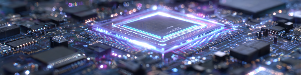
Synopsys and TSMC Deepen AI Chip Design Partnership: Key Takeaways
Synopsys and TSMC expanded their collaboration to better align IP, AI-driven EDA, and leading-edge manufacturing. The goal is faster delivery of high-performance computing and AI chips by optimizing design, verification, and manufacturability together.
What Was Announced
- Interface IP for advanced nodes (3nm and 2nm-class): Silicon-proven IP including M-PHY v6.0 (low-power bring-up on N2P), plus ongoing tapeouts for 64G UCIe and 224G high-speed interconnect.
- AI-enhanced EDA flows: More proactive AI optimization in certified flows, including “run assistance” in Fusion Compiler with TSMC’s A14 and NanoFlex Pro, targeting better PPA and higher productivity.
- Advanced packaging and system integration: 3DIC Compiler support for TSMC CoWoS, including large interposers (up to 5.5× reticle), backed by multiphysics simulation (thermal, electrical, optical).
- New market expansion: Automotive UCIe IP meeting ASIL B on N5A, plus continued M-PHY progress for mobile and storage.
- AI infrastructure with CPO: Multiphysics support for co-packaged optics via TSMC COUPE, paired with 224G IP for optical Ethernet and interconnect standards such as UALink.
Why It Matters
- AI systems are increasingly limited by data movement, power, and integration, not just compute.
- Tighter coupling of IP, EDA, packaging, and process reduces risk and can shorten schedules.
- More “agentic” AI in EDA could shift optimization work from engineers to AI systems.
Market Implications
- Strengthens Synopsys’s position as an AI-silicon enabler and reinforces TSMC’s ecosystem.
- Certified node-specific flows raise switching costs, increasing strategic advantage for tightly integrated partners.
发表回复
要发表评论,您必须先登录。