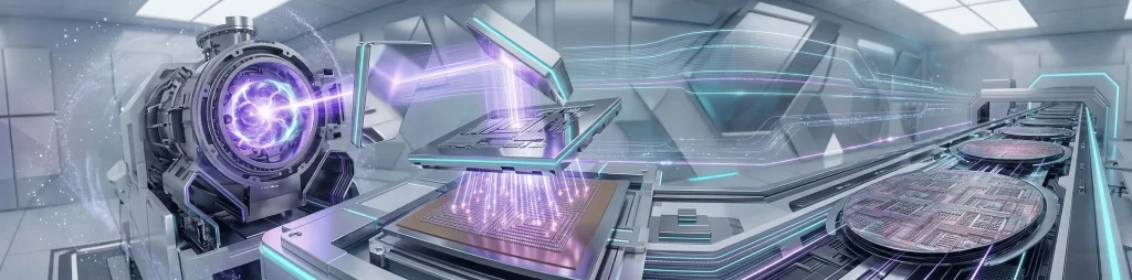
The semiconductor industry is entering a pivotal inflection point. As chipmakers race toward the 2 nm node and beyond, High-NA EUV lithography is transitioning from R&D curiosity to production-qualification reality. But the scanner itself is only one piece of a far larger puzzle. Masks, photoresists, etch, deposition, metrology, and yield management each present distinct bottlenecks that will determine how quickly — and how profitably — High-NA EUV can reach high-volume manufacturing.
Why High-NA EUV Matters Now
Extreme ultraviolet (EUV) lithography at 0.33 numerical aperture (NA) has been the workhorse of leading-edge patterning since its commercial debut around the 5 nm node. However, as design rules shrink below 13 nm half-pitch, the resolution limits of 0.33 NA optics force chipmakers into costly multi-patterning schemes — multiple mask exposures, additional etch and deposition steps, and tighter overlay budgets.
High-NA EUV, with a numerical aperture of 0.55, pushes single-exposure resolution down to approximately 8 nm half-pitch. ASML’s TWINSCAN EXE:5000, the first High-NA prototype scanner, has been operational at imec and Intel since 2024. In late 2025, Intel installed the industry’s first commercial-grade EXE:5200B, which passed acceptance testing for development of the Intel 14A process node.
By February 2026, ASML publicly confirmed that its High-NA EUV tools have processed over 500,000 silicon wafers and achieved uptime above 80%, signaling technical readiness for volume production. The company’s CTO noted that full integration into manufacturing lines is expected within 2–3 years, placing the mass-production inflection squarely in the 2027–2028 window.
Yet readiness of the scanner alone does not equal readiness of the ecosystem. The bottleneck map stretches across the entire patterning stack.
How Does the Anamorphic Optical Design Change the Game?
The jump from 0.33 NA to 0.55 NA is not a simple lens swap. The higher numerical aperture means photons strike the mask and wafer at steeper angles, introducing severe 3D mask effects — shadowing within the absorber layer that degrades image contrast.
ASML and Carl Zeiss SMT addressed this with an anamorphic optical design: the demagnification ratio changes from the traditional 4×/4× to 4×/8×. In the scanning direction, the mask image is reduced by 8×, which halves the effective field size at the wafer. This means the printable area per exposure is roughly half that of a 0.33 NA scanner (a half-field of approximately 26 mm × 16.5 mm versus the full 26 mm × 33 mm field).
The consequences ripple outward:
- Throughput pressure: Fewer dies per exposure pass. ASML compensates with faster wafer and reticle stages, plus a higher-power EUV source, but the net throughput of the EXE:5200B still trails the mature NXE:3800E in wafers per hour.
- Mask compatibility: The 4×/8× demagnification demands new mask layouts. Existing 4×/4× reticle designs cannot be reused directly. Mask data preparation, optical proximity correction (OPC), and inverse lithography technology (ILT) flows must all be updated.
- Stitching: For dies larger than the half-field, field stitching is required — a non-trivial overlay and yield challenge.
What Are the Critical Mask Bottlenecks?
Anamorphic Mask Manufacturing
The shift to 4×/8× demagnification fundamentally changes mask geometry. Features in the scan direction are magnified by 8× on the reticle, while features in the cross-scan direction remain at 4×. This anamorphic distortion complicates every step of mask fabrication — from e-beam writing to pattern inspection and repair.
Intel presented at SPIE 2025 on the progress of anamorphic mask manufacturing, covering critical processes including patterning, inspection (with and without pellicle), review, repair, and registration correction. The conclusion: while feasible, the process requires tighter control of placement error and new inspection algorithms tuned to the asymmetric geometry.
Curvilinear Mask Patterns and ILT
As feature sizes shrink, traditional Manhattan (rectilinear) mask shapes are increasingly inadequate. Curvilinear masks generated via inverse lithography technology (ILT) deliver superior process windows and better across-pitch performance. However, writing curvilinear patterns with conventional variable-shaped beam (VSB) e-beam writers is prohibitively slow — write times can increase by 5–10× compared to Manhattan patterns.
Multi-beam mask writers, such as those from IMS Nanofabrication (now part of KLA), are critical enablers. They can write curvilinear patterns without the shot-count penalty of VSB tools. But the installed base of multi-beam writers is still limited, and the infrastructure for full-chip curvilinear tapeout — including mask rule checks, data handling, and repair — remains an area of active development.
Pellicle Readiness
EUV pellicles protect the mask surface from particle contamination during exposure. For 0.33 NA EUV, pellicle adoption has been gradual but is now approaching maturity. For High-NA, the challenge intensifies: the wider angular cone of the 0.55 NA optics requires pellicles with higher EUV transmittance and greater thermal resilience, as the increased angular spread concentrates more heat on the pellicle membrane.
ASML and partners are developing next-generation pellicles, but the qualification timeline for High-NA-compatible pellicles remains a gating factor for production insertion.
Why Are Photoresists the Most Talked-About Bottleneck?
The Resolution–Sensitivity–Roughness Triangle
Photoresists for EUV lithography face a fundamental tradeoff known as the RLS triangle: Resolution, Line-edge roughness (LER), and Sensitivity. Improving any two parameters typically degrades the third. At High-NA dimensions — 8–10 nm half-pitch — this tradeoff becomes acute.
The higher NA optics require thinner resist films (typically below 30 nm) to maintain adequate depth of focus and avoid pattern shadowing. Thinner resists absorb fewer photons, exacerbating photon shot noise — the root cause of stochastic defects.
Stochastic Defects: The Yield Killer
Stochastic defects — random, non-repeating failures such as microbridges, line breaks, and missing contacts — are arguably the single greatest threat to High-NA EUV yield. These defects arise from the statistical nature of photon absorption and chemical reactions at the nanometer scale.
Research from imec and Fractilia has shown that stochastic defects scale with the square root of dose: doubling the exposure dose reduces stochastic failures, but at the cost of halving throughput. At production-relevant doses (typically 30–60 mJ/cm²), the stochastic “cliff” — the dose threshold below which defect rates spike exponentially — is dangerously close to the operating window.
Metal Oxide Resists vs. Chemically Amplified Resists
Two resist platforms are competing for High-NA EUV:
- Chemically amplified resists (CARs): The incumbent technology. CARs rely on acid diffusion to amplify the chemical change initiated by photon absorption. However, at sub-10 nm features, acid diffusion introduces pattern blur that fundamentally limits resolution.
- Metal oxide resists (MORs): Inorganic resists based on tin-oxo or similar metal-oxide clusters. MORs offer a higher EUV photon absorption cross-section (capturing more photons per unit volume) and undergo chemical changes without diffusion, delivering sharper pattern edges. Lam Research’s dry-deposited resist platform and JSR/Inpria’s spin-on MOR are leading candidates.
Early data from Lam Research showed that dry resist achieves a significant failure-free process window at 26–28 nm pitch, a promising sign for High-NA insertion. Meanwhile, non-PFAS biomass-based EUV resists have demonstrated patterning capability at 8 nm in 0.50 NA configurations, pointing toward more sustainable material options.
No clear winner has emerged. The industry may ultimately adopt different resist platforms for different layers, adding complexity to the manufacturing flow.
How Do Etch and Deposition Adapt to High-NA Requirements?
Ultra-Thin Resist and Etch Transfer
Thinner resist layers — a necessity for High-NA depth-of-focus requirements — provide less etch budget. The resist erodes faster during pattern transfer, narrowing the process window for critical dimension (CD) control. This drives demand for:
- Harder underlayer stacks: Carbon-based or metal-containing hardmasks that can withstand aggressive etch chemistries while faithfully transferring the resist pattern.
- Atomic layer etching (ALE): Precise, self-limiting etch processes that remove material one atomic layer at a time, minimizing CD variation and improving line-edge roughness post-etch.
Deposition Challenges
Advanced nodes increasingly rely on atomic layer deposition (ALD) for conformal thin-film coverage in high-aspect-ratio structures. For High-NA EUV layers — particularly metal interconnect and contact layers — the requirements include:
- Sub-angstrom thickness uniformity across the wafer.
- Low-temperature processes compatible with thermally sensitive resist underlayers.
- Novel barrier and liner materials (e.g., ruthenium, molybdenum) to replace copper dual-damascene schemes at the tightest pitches.
Equipment suppliers like Lam Research, Applied Materials, and Tokyo Electron are developing new etch and deposition modules specifically optimized for the thinner films and tighter tolerances of High-NA patterning layers.
What Metrology Gaps Must Be Closed?
In-Line CD and Overlay Measurement
At 8 nm half-pitch, the allowable CD variation shrinks to sub-nanometer levels. Traditional optical CD metrology (OCD/scatterometry) faces signal-to-noise challenges at these dimensions. CD-SEM (critical dimension scanning electron microscopy) remains essential but must contend with:
- Resist shrinkage under electron beam exposure, which biases measurements.
- Throughput limitations when full-wafer mapping is required for stochastic defect monitoring.
Overlay — the alignment accuracy between successive patterning layers — must be controlled to within 1–2 nm for High-NA layers. This demands next-generation alignment and overlay metrology tools with sub-0.5 nm measurement uncertainty.
Stochastic Defect Inspection
Detecting stochastic defects at High-NA dimensions is a metrology challenge in its own right. These defects are random and non-repeating, meaning traditional die-to-die or die-to-database inspection strategies may miss them. New approaches include:
- High-throughput e-beam inspection for detecting buried and surface stochastic defects.
- Machine-learning-based defect classification to distinguish true stochastic failures from measurement noise.
- Stochastic simulation and prediction models that correlate resist chemistry, dose, and process conditions to defect probability — enabling virtual inspection and process optimization.
KLA, ASML (via its HMI subsidiary), and Applied Materials are all investing heavily in next-generation inspection and metrology platforms targeting the High-NA ecosystem.
How Will Yield Management Evolve?
Yield is the ultimate arbiter of High-NA EUV’s economic viability. Early yield data from Intel, presented at SPIE 2025, showed that High-NA contact-hole layers achieved comparable yield to mature low-NA multi-patterning processes — an impressive result given the early stage of mask and process optimization.
However, several yield risks remain:
- Stochastic yield loss: Even at parts-per-billion defect rates, the sheer number of features on an advanced chip means stochastic defects can dominate the yield budget.
- Overlay-driven yield loss: Tighter overlay requirements between High-NA and low-NA layers (or between High-NA stitched fields) require advanced feed-forward and feedback control loops.
- Mask-induced yield loss: Mask defects, phase errors from multilayer roughness, and pellicle-related issues all contribute to systematic yield detractors.
Yield management systems must integrate data from lithography, etch, deposition, and metrology tools into holistic process control frameworks — often powered by AI and machine learning — to identify and correct yield-limiting excursions in real time.
Who Is Leading the High-NA EUV Race?
The competitive landscape is taking shape:
- Intel has been the most aggressive early adopter, installing both the EXE:5000 (R&D) and EXE:5200B (production-qualification) tools. Intel’s 14A node is expected to be the world’s first process to use High-NA EUV on critical layers.
- Samsung and SK hynix are investing in High-NA for both logic and advanced DRAM (sub-10 nm DRAM patterning), with production use targeted for 2027–2028.
- TSMC, traditionally conservative in adopting new lithography generations, is evaluating High-NA but may defer production insertion until the ecosystem is more mature, relying on continued optimization of 0.33 NA multi-patterning in the interim.
The equipment and materials supply chain — ASML, Carl Zeiss SMT, Lam Research, Tokyo Electron, JSR, Shin-Etsu, Mitsui Chemicals, KLA, and others — is racing to qualify their respective pieces of the puzzle.
What Comes After High-NA EUV?
Looking further ahead, the industry is already exploring Hyper-NA concepts (NA > 0.55) and alternative patterning approaches such as directed self-assembly (DSA) and nanoimprint lithography (NIL). ASML has disclosed early investigations into extending the EUV roadmap beyond 0.55 NA. However, these remain long-term research topics — the immediate priority is making 0.55 NA High-NA EUV work reliably and economically in the 2027–2028 production window.
Key Takeaways
- High-NA EUV scanners are production-ready. ASML’s EXE:5200B has passed acceptance testing and processed over 500,000 wafers with 80%+ uptime.
- Masks are a critical bottleneck. Anamorphic layouts, curvilinear ILT, multi-beam writing, and High-NA pellicles all require further maturation.
- Photoresists remain the most debated challenge. Metal oxide resists and dry resists show promise, but no single platform has won the resolution–sensitivity–roughness tradeoff.
- Etch, deposition, and metrology must co-evolve. Thinner resists demand harder underlayers, atomic-layer precision, and sub-nanometer measurement capability.
- Yield management is the ultimate gatekeeper. Stochastic defects, overlay control, and mask quality will determine High-NA’s economic viability at scale.
The transition to High-NA EUV is not a single technology bet — it is a synchronized ecosystem upgrade. The companies that align their scanner, mask, resist, etch, deposition, metrology, and yield strategies will define the next generation of semiconductor manufacturing.
发表回复
要发表评论,您必须先登录。