The 224 Gbps PAM4 electrical lane is no longer a laboratory curiosity. OIF’s CEI-224G family — spanning XSR (on-package), VSR (chip-to-module), MR (chip-to-chip), and LR (backplane / copper cable) — is the architectural anchor for 1.6T Ethernet, PCIe Gen7, NVLink 6, UALink, CXL next-gen, and 448G roadmap demonstrations.[1] Every hyperscaler building scale-up and scale-out AI fabrics in 2026 is forced to validate 224G backplane connectors at a level of precision that didn’t exist two generations ago.
Why does it matter so much? Because at 224 Gbps PAM4, the channel budget is brutally thin. Keysight’s March 2026 launch of an end-to-end 1.6T / 224G validation portfolio explicitly frames the problem as “signal integrity at extreme data rates, tighter compliance margins, and the need for efficient, repeatable testing in high-volume manufacturing.”[2] At these speeds, a micron-scale mechanical deformation in a connector’s mating interface — a bent compliant pin, a resin-rich region in a press-fit, a tolerance stack-up in a wafer lock — translates directly into an impedance discontinuity that eats eye height, lifts return loss above mask, and drives the FEC margin to zero.
What is actually flowing through the connector?
- Symbol rate: ~112 GBd PAM4 ⇒ Nyquist ≈ 53.125 GHz.[3]
- Useful measurement bandwidth: typically up to 67 GHz minimum, with leading-edge labs pushing 90–110 GHz S-parameter capture for channel extraction.[4]
- System reference impedance: differential 85 Ω or 92 Ω for most modern SerDes (Socionext’s 2026 224G/448G package study targets 92.5 Ω differential), with OIF also simulating 90 Ω vs 100 Ω as a tuning trade-off for VSR channels.[5][6][7]
- Impedance tolerance: IEEE P802.3df 224G package/PCB studies verify interconnects to ±10% of target differential impedance (e.g., 80 Ω ±10%) — that is the practical envelope inside which a modern backplane connector must stay across its entire mating interface, footprint, and via field.[8]
Ten percent sounds generous until you remember that a single connector pair typically stacks contributions from compliant-pin compression, resin-rich voids around press-fit eye-of-the-needle contacts, footprint capacitance, anti-pad geometry, PCB via stubs, and cable termination. Each one nudges the TDR trace. Impedance matching at 224G is the integral of a dozen small mechanical and dielectric uncertainties — and any one of them going out of spec is enough to kill the link.
How Do You Actually Measure a 224G Backplane Connector?
This is where test-instrument requirements become extreme. A 2026 connector evaluation lab typically needs the following stack — and each tier materially raises cost and calibration difficulty.
1. Vector Network Analyzer (VNA) for S-parameters
The VNA is the reference instrument. For CEI-224G compliance work, engineers extract mixed-mode S-parameters (SDD11, SDD21, SCD21, etc.) out to at least the second harmonic of Nyquist. TRS-RenTelco’s 224G characterization study shows that cutting VNA bandwidth from 90 GHz down to 67 GHz noticeably shifts the predicted COM (Channel Operating Margin), and moving from a 1.85 mm connector setup (67 GHz) to a 1.0 mm setup (110 GHz) roughly triples the cost of cables, calibration kits, and the VNA itself.[4]
For 224G backplane connector characterization specifically, practical guidance from IEEE and OIF contributions emphasizes:
- De-embedding test fixtures and launch structures using 2x-thru / AFR / IEEE 370-class methods.
- Narrow IF bandwidth to recover low-level crosstalk terms (NEXT/FEXT below −60 dB).[9]
- Verifying that the connector footprint, via, and anti-pad geometry stay inside the target differential impedance envelope (commonly 85 Ω or 92 Ω) up to ~50 GHz, with controlled roll-off beyond.
2. Time-Domain Reflectometry (TDR) for spatial impedance resolution
Where the VNA tells you “how much energy reflects,” the TDR tells you “where it reflects from.” That spatial view is indispensable for backplane connector debug because it localizes impedance discontinuities to the mating interface, the press-fit tail, the via transition, or the PCB trace launch.
Modern 224G-class TDRs such as MultiLane’s Pulsar use rise times around 7–12 ps and run 4 lanes in parallel for production testing of switch ports, cables, and connectors — the kind of throughput a 224G backplane assembly line actually demands.[10] IEEE P802.3df package verification work shows TDR confirming 80 Ω differential ±10% across skip-layer and regular routing designs, demonstrating that TDR is still the primary acceptance check for impedance uniformity at 224G.[8]
3. High-bandwidth real-time oscilloscopes + BERT for COM / eye / jitter
Compliance to CEI-224G-MR and CEI-224G-LR requires real-time scopes and PAM4 BERTs capable of capturing PRBS13Q patterns and computing Jnu, JRMS, EOJ, SNDR, linear fit pulse ratio, effective return loss, and COM. Keysight’s D9020224C test application automates nearly 100 electrical compliance tests for the 224G transmitter mask alone.[11]
4. IBIS-AMI + COM correlation
Because 224G channels are FEC-protected and equalization-heavy, pure frequency-domain pass/fail is insufficient. Engineers increasingly correlate measured S-parameters against IBIS-AMI models and run statistical channel analysis (MathWorks’ CEI-224G-MR compliance kit and Serial Link Designer are representative of this workflow).[12] The output — Eye Height, Vertical Eye Closure, COM — is what connector vendors ultimately publish in their 224G datasheets.
Question: Can I just reuse my 112G test bench?
Short answer: no. A 112G-class setup typically tops out at 40–50 GHz VNA, 50 Ω SMA/2.92 mm launches, and TDRs with ~20 ps rise times. At 224G, crosstalk floors are −125 dB at 56 GHz for well-designed package traces, the fixture launch itself becomes a dominant error source, and calibration kit drift over hours-long S-parameter sweeps can erase the 1–2 dB margin you’re trying to measure.[8] Expect to refresh the calibration kit to 1.0 mm or 0.8 mm, requalify every cable, and in many cases buy a new VNA.
The 2026 Backplane Connector Landscape: Who Is Shipping What?
Rather than recycling marketing claims, here’s what the major vendors have publicly committed to for 224G backplane and cabled-backplane interconnects. This matters for the editorial angle because impedance-fluctuation testing only becomes concrete once you know the mechanical architectures engineers are actually evaluating.
Amphenol — ExaMAX2® / PaladinHD2® / OverPass™ / ZettaMAX™
Amphenol Communications Solutions positions its OverPass™ cabled backplane with PaladinHD2® and ExaMAX2® connector families as the passive-copper reach-extender for 224G PAM4, with a roadmap into PCIe 7.0.[13] At DesignCon 2026, Amphenol introduced ZettaMAX™, a next-generation high-speed backplane platform engineered for 224G and positioned against future 300G performance.[14][15] Amphenol-BSI separately confirms 224 Gb/s traditional backplane technology with simulations and test reports scheduled for partner release in 2026.[16]
TE Connectivity — AdrenaLINE® Slingshot 224G HD
TE’s AdrenaLINE® Slingshot high-density 224G backplane solution guide explicitly advertises 67 GHz bandwidth margin for 224G Ethernet, PCIe Gen 6/7, NVLink 6, InfiniBand, UALink, and CXL — a clear signal that the connector has been characterized well beyond Nyquist to leave headroom for channel variation.[17] The portfolio spans near-chip, cabled backplane, cabled I/O, and in-house 224G twinax cable, reflecting the industry’s pivot from traditional PCB-routed backplanes to cabled backplane architectures where the connector-to-cable launch becomes the dominant impedance-control problem.[18]
Samtec — Si-Fly® HD Backplane
Samtec’s Si-Fly® HD cable backplane system hits up to 2,048 differential pairs per open rack unit and an aggregate 7.2 Tbps per 64-pair connection, enabled by Eye Speed® hyper-low-skew twinax (≤ 1.75 ps/m max intra-pair skew).[19] Samtec publicly demonstrated a zero-error loopback through the Si-Fly HD cable backplane driven by Synopsys 224G PHY IP in April 2026.[20] That demo is essentially an end-to-end empirical answer to the impedance-fluctuation question: the link works because the connector’s mating interface and cable launch hold impedance tightly enough that the PHY’s DFE/FFE has margin to close the eye.
Molex — CX2 Dual-Speed 224G
Molex frames the 224G interconnect problem as near-ASIC chip-to-chip, arguing that low-loss twinax cabling plus a shielded high-density interface outperforms PCB traces at 224G for the short-reach chip-to-chip channel.[21] The testing implication: the connector-to-cable impedance match must be characterized as a single system, because separating the two artificially hides reflections that only appear when they’re mated.
Where is the market gap?
Scanning competitor content for whychip.com editorial positioning, three gaps stand out:
- Vendor datasheets rarely publish full mating-interface TDR under mechanical stress. Most show nominal insertion/return loss but not impedance fluctuation vs. mating force, mating cycles, thermal soak, or off-axis misalignment. That is precisely the data SI engineers need to predict real-world link yield at 224G.
- Few independent write-ups cross-reference OIF CEI-224G-LR reference channels, IEEE P802.3df package studies, and shipping vendor connector families in one place. Practitioners have to assemble the picture themselves.
- Manufacturing-side test — parallel 4-lane TDR, production BERT, automated compliance reporting — is under-covered versus R&D characterization. As 224G goes into volume, this is where the pain will shift.
This article deliberately sits in that gap.
Root Causes of Impedance Fluctuation in 224G Backplane Connectors
At 224 Gbps, impedance fluctuation is not one problem — it is a superposition of at least seven mechanisms. Understanding each is how you design a test plan that actually catches defects.
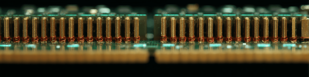
1) Mechanical deformation of compliant contacts
Compliant-pin and eye-of-the-needle press-fit contacts rely on controlled interference with the PCB through-hole. Over-insertion, under-insertion, hole plating variation, or resin-rich zones change contact force and contact area, which in turn change local inductance and capacitance. At 224G, a few micrometers of geometry change is enough to shift the local differential impedance by several ohms.
2) Mating-interface wiping and wear
Gold/palladium plating wear after repeated mate/unmate cycles alters skin-depth behavior around Nyquist (53 GHz) and second harmonic (~67–110 GHz). Skin depth scales as √(1/f), so the copper microstructure at the contact — including roughness and plating morphology — dominates loss and local reflections at 224G in a way that was negligible at 25 Gbps NRZ.[5]
3) Via stubs and footprint anti-pads
TestConX 2025 guidance is explicit: vias for 224G must be optimized with a 3D field solver (HFSS, CST) and tuned to the target 85 Ω or 92 Ω by adjusting drill diameter and copper keep-outs; the historical sweet spot for well-tuned through-hole via impedance is ~45–50 GHz of usable bandwidth — right at the edge of what 224G demands.[5] Back-drilling depth tolerance, remaining-stub length, and anti-pad diameter are all first-order impedance-fluctuation contributors.
4) PCB material & copper roughness
Low-Dk, low-Df materials plus VLP (very-low-profile) copper are table stakes, but even then, conductor loss models such as the Huray and Cannonball roughness models (the latter recognized at DesignCon 2026) are required to predict measured vs. simulated correlation inside ±1 dB at 50+ GHz.[22]
5) DC-blocking capacitors in the link
Discrete DC-blocking caps, historically innocuous, introduce visible impedance discontinuities at 224G. A DesignCon paper on evaluating 224G SI performance of DC-blocking caps warns that treating the cap as a simple lumped element “could lead to incorrect conclusions since the DC blocking cap may yield significant impedance mismatches.”[23] For backplane connector evaluation, you must include the AC-coupling cap in the test fixture de-embed strategy, not pretend it’s ideal.
6) Package / BGA transition
Socionext’s 2026 whitepaper on 224G/448G package analysis targets 92.5 Ω differential, uses 0.8 mm ball pitch, 20 buildup layers, and explicitly calls out that bump pads, substrate BGA, and top-side pads must be routed separately with Near Package Copper / Co-Packaged Copper in mind.[6] The backplane connector does not see the SerDes directly — it sees the full package-to-board transition, and that transition’s impedance ripple is part of what the connector test has to tolerate.
7) Return loss weighting vs. insertion loss
The OIF CEI-224G framework document is explicit that at 224 Gbps, return loss weighs more heavily in low-loss channels than it did at 112 Gbps, and channel metrics need to reflect that.[7] Practically, this means a connector with slightly higher insertion loss but tighter impedance control may outperform a lower-loss connector with ripple — a reversal of the 112G-era design intuition.
A Practical Test Recipe for Evaluating a New 2026 Backplane Connector
Here is a pragmatic flow that a signal-integrity team can adopt, combining the best practices from OIF, IEEE P802.3df, TestConX, and the major vendors:
- Define the system reference impedance (typically 85 Ω, 92 Ω, or 92.5 Ω differential) and lock it at the SerDes, package, connector, and PCB levels. Do not mix.
- Design a 2x-thru test fixture with SMA / 1.85 mm / 1.0 mm launches matched to the VNA calibration kit. Target fixture return loss better than −20 dB to 67 GHz (stretch: 90 GHz).
- Measure mixed-mode S-parameters (SDD11, SDD21, SCD21, SCC11) with narrow IF bandwidth. Verify IL, RL, NEXT, FEXT against CEI-224G-LR masks.
- Run 4-port TDR with ≤12 ps rise time to localize discontinuities. Accept the connector region within ±10% of target differential impedance.
- De-embed the fixture using IEEE 370 / AFR methods. Re-verify that the extracted connector-only S-parameters pass mask.
- Mechanical stress testing: repeat TDR after N mate/unmate cycles, thermal soak, and deliberate off-axis alignment. Look for impedance drift — this is the “micro-deformation” acceptance criterion.
- COM / IBIS-AMI correlation: feed extracted S-parameters into a CEI-224G-LR or CEI-224G-MR compliance kit. Require COM margin ≥ target (typically ≥ 3 dB) across corner cases.
- Production gate: move to automated 4-lane TDR systems (MultiLane Pulsar-class) and PAM4 BERTs with automated compliance reports for high-volume test.[10]
Frequently Asked Questions
What makes 224G SerDes testing harder than 112G?
Nyquist roughly doubles (from ~28 GHz to ~53 GHz), useful test bandwidth stretches from 40 GHz to 67–110 GHz, return loss becomes weighted more heavily than insertion loss, and FEC-protected PAM4 demands statistical COM-based acceptance rather than simple mask pass/fail.[7][4]
What is the typical impedance target for a 224G backplane connector?
85 Ω or 92 Ω differential is common for SerDes, with 92.5 Ω used in some 2026 package studies; practical tolerance is ±10% across the full connector + via + footprint assembly.[5][8][6]
Are cabled backplanes replacing traditional PCB backplanes at 224G?
Increasingly yes, especially for reach beyond ~20 inches. Amphenol OverPass, TE AdrenaLINE Slingshot, Samtec Si-Fly HD, and Molex CX2 all point to twinax-cabled architectures where the connector-to-cable launch replaces long PCB traces as the dominant impedance-control surface.[13][17][19][21]
Do I need a 110 GHz VNA?
Not always. 67 GHz is the practical minimum for CEI-224G work. Going to 90–110 GHz improves channel extraction fidelity and is the direction the industry is moving, but triples the cost of cables, calibration kits, and the VNA itself.[4]
Is TDR still relevant when VNA + COM can model everything?
Yes. TDR remains the fastest way to spatially localize an impedance discontinuity to the mating interface, press-fit, via, or launch — information a scalar COM number hides. IEEE P802.3df continues to use TDR for package and PCB impedance verification at 224G.[8]
Takeaways for Hardware Architects Buying 224G Connectors in 2026
- Ask vendors for TDR traces under mechanical stress and after mating cycles, not just nominal S-parameters.
- Demand explicit CEI-224G-LR / CEI-224G-MR COM margin data, with the reference channel disclosed.
- Verify the vendor’s impedance target matches your SerDes (85 Ω vs 92 Ω vs 92.5 Ω differential). Mixing is where silent failures happen.
- Budget early for 1.0 mm or 0.8 mm calibration kits and 90+ GHz VNAs if you plan to second-source connectors or qualify multiple PCB stack-ups.
- Treat cabled backplane launches and DC-blocking caps as first-class impedance-control elements, not afterthoughts.[23]
At 224 Gbps, the connector is no longer a passive commodity. It is a precision microwave component whose mechanical tolerances, plating, and footprint together decide whether a 1.6T link closes. The labs and vendors that publish honest, mechanically-stressed impedance data will win the 2026 design-in cycle.
发表回复
要发表评论,您必须先登录。