The explosive growth of artificial intelligence is forcing a complete rethink of computer chip design. As AI models balloon to trillions of parameters, simply making transistors smaller isn’t enough anymore. The industry is pivoting to a new frontier: system-level innovation. The future of AI performance now hinges on how well entire systems—compute, memory, and power—are integrated together, a shift where advanced packaging and 3D integration are taking center stage.
Beyond the Transistor: The Era of System-Level Design
The demand for AI computing power is skyrocketing, far outpacing what traditional chip scaling can deliver. This has created a critical performance gap. The key insight is that AI performance is no longer just about the silicon chip itself; it’s about the entire system. Future breakthroughs will depend on seamlessly weaving together processing, memory, and data pathways into a unified, efficient package. This marks a move from focusing on individual components to a holistic, full-stack design philosophy.
Confronting AI’s Core Challenges
To understand why this shift is necessary, we must look at the fundamental bottlenecks holding back today’s AI hardware.\n\n
1. The Data Movement Problem
In modern AI systems, the biggest constraint often isn’t raw computation—it’s moving data around. Shuttling information between separate chips can use up to 50 times more energy than moving it within a single chip. Furthermore, waiting for data can leave powerful processors idle, drastically reducing efficiency. This makes the design of high-speed, low-energy interconnects a top priority.\n\n
2. The Growing Memory Wall
AI models are becoming memory-hungry at an even faster rate than they are compute-hungry. New applications, like processing long documents or combining text and images, require massive amounts of fast memory. We’re moving from needing gigabytes to needing terabytes of capacity, all with minimal delay. Since memory technology isn’t advancing as quickly as processing technology, this “memory wall” is a major hurdle. Breaking through it requires innovative ways to integrate vast amounts of high-speed memory directly with processors.
3. The Power and Heat Ceiling
Packing more computing power into smaller spaces, especially with 3D stacking, leads to intense heat and soaring power demands. These factors are now primary limits on how far we can scale AI systems. Without major leaps in power efficiency and cooling solutions, performance gains will stall. Managing power and thermals is no longer a back-end task—it’s a core design challenge from the very beginning.\n\n
TSMC’s Technological Response: Building the Foundation
To tackle these interconnected challenges, foundries like TSMC are pioneering new integration technologies that act as the foundation for next-generation AI.\n\n
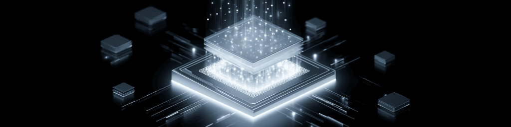
3D Fabric: The Integration Backbone
TSMC’s 3D Fabric technologies are a suite of solutions designed to combine multiple chips into a single, high-performance system. Techniques like 3D chip stacking create incredibly dense vertical connections, slashing the distance data must travel and saving significant energy. Advanced packaging platforms, such as CoWoS, allow logic chips (the brains) and memory chips to be placed side-by-side with extreme proximity. This enables massive leaps in data bandwidth and capacity. Through these methods, the package around the chips transforms from a passive container into an active, performance-defining element of the system.\n\n
Co-Packaged Optics: A Faster, Cleaner Connection
As traditional electrical wires reach their speed and efficiency limits, a new solution is emerging: co-packaged optics (CPO). This approach integrates tiny light-based (optical) communication modules right next to the compute chips. Light can transmit data much faster and with far less power loss over distance than electricity. For data centers connecting thousands of AI servers, CPO offers a scalable path to higher bandwidth and radically improved energy efficiency.\n\n
System-on-Wafer: The Ultimate Integration
Looking to the future, integration is moving toward wafer-scale. Imagine building an entire server’s worth of components on a single, dinner-plate-sized silicon wafer, instead of cutting it into hundreds of individual chips. This System-on-Wafer (SoW) concept minimizes the slow, inefficient connections between discrete packages. By keeping communication paths extremely short on a unified substrate, it promises unprecedented levels of performance and efficiency for the most demanding AI workloads.
The Holistic Approach: System Technology Co-Optimization (STCO)
With AI systems becoming so complex, optimizing one part in isolation—like just the chip design or just the packaging—is ineffective. This has given rise to System Technology Co-Optimization (STCO). STCO is a design philosophy where chip architecture, packaging choice, interconnect strategy, power delivery, and cooling are all considered simultaneously from the start. This ensures every part of the system is designed to work in perfect harmony, maximizing overall performance and energy savings. It represents a fundamental change in how complex hardware is created.
The Road Ahead: The System Is the New Chip
The trajectory for AI hardware is clear. Progress will be driven less by microscopic transistor scaling and more by macroscopic system integration. Advances in advanced packaging, optical interconnects, memory architectures, and power management must converge through intelligent, system-level design. In this new paradigm, the complete, integrated system itself becomes the primary unit of innovation. Success will belong to those who can master this full-stack co-design. As this transformation unfolds, one thing is certain: in the age of AI, the system has effectively become the new chip.
发表回复
要发表评论,您必须先登录。