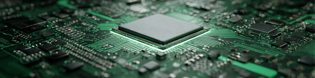
Introduction: The “Power Wall” of the AI Era
As we enter late 2025, the proliferation of Generative AI has pushed data center physical infrastructure to its limits. With the deployment of gigawatt-scale “AI Factories” and rack power densities soaring past 100kW (driven by architectures like NVIDIA Blackwell NVL72), the traditional power delivery network (PDN) is facing an existential crisis. The industry is aggressively pivoting from 12V to 48V architectures to combat $I^2R$ losses, but copper and voltage alone are not enough. The spotlight has turned to the semiconductors switching these massive currents: Gallium Nitride (GaN) and Silicon Carbide (SiC).
For hardware engineers, procurement managers, and system architects, the choice between GaN and SiC is no longer just about “Wide Bandgap” hype—it is a critical selection decision driven by specific voltage nodes, thermal constraints, and reliability data. This article provides a comprehensive, data-driven analysis of where each material wins in the AI power chain, from the grid interface down to the GPU core.
1. The Physics of the Duel: Why Silicon Can’t Keep Up
To understand the “Protagonist” battle, we must first look at the atomic level. Both GaN and SiC far outperform traditional Silicon (Si) MOSFETs and IGBTs, but they do so in different ways.
1.1 Material Properties Comparison
| Property | Silicon (Si) | Gallium Nitride (GaN) | Silicon Carbide (SiC) | Impact on AI Power |
|---|---|---|---|---|
| :— | :— | :— | :— | :— |
| Bandgap (eV) | 1.1 | 3.4 | 3.3 | Both withstand higher voltages and temperatures than Si. |
| Electron Mobility ($mu$) | 1300 | 2000 | 650 | GaN wins. Higher mobility means faster switching speeds (MHz range) and lower On-Resistance ($R_{DS(on)}$). |
| Thermal Conductivity (W/mK) | 150 | 130 | 490 | SiC wins. Superior heat dissipation makes SiC ideal for high-temperature, high-power environments. |
| Critical Electric Field (MV/cm) | 0.3 | 3.3 | 3.0 | Both allow for thinner drift regions, enabling smaller devices with lower resistance. |
The Verdict: GaN is the “Sprinter”—unbeatable speed and efficiency at lower voltages (<650V). SiC is the “Marathon Runner”—robust, thermally stable, and dominant at high voltages (>900V).
2. The Battlefield: Mapping the AI Power Delivery Network (PDN)
An AI data center PDN is not a monolith; it is a multi-stage conversion chain. The “protagonist” changes depending on where you look in the chain.
2.1 The Front End: AC-DC and Grid-to-Rack (SiC’s Stronghold)
At the entrance of the server rack (or the power shelf), 3-phase AC power (typically 415V or 480V) must be converted to 48V DC. This stage requires handling high voltages and substantial power (3kW to 5.5kW per PSU module, paralleled for 100kW+ racks).
- Topology: Totem-Pole PFC (Power Factor Correction) or Vienna Rectifiers.
- Why SiC Wins Here:
- Voltage Headroom: 1200V SiC devices provide ample safety margin for 480V AC inputs, whereas 650V GaN is pushed to its limit or requires complex multilevel topologies.
- Thermal Robustness: In the hot aisle of a data center, PSUs run hot. SiC’s superior thermal conductivity simplifies cooling.
- Avalanche Ruggedness: Grid power is dirty. SiC has inherent avalanche capability to absorb surges; GaN HEMTs typically do not (though protection circuits can mitigate this).
- 2025 Trend: Moving to 800V DC distribution (promoted by NVIDIA and others). In an 800V backbone, 1200V-1700V SiC MOSFETs are the undisputed kings, as GaN technology at these voltages is not yet commercially mature for high-power commodity applications.
2.2 The “Last Inch”: 48V to Load (GaN’s Dominion)
This is the critical “Vertical Power Delivery” zone. The 48V busbar delivers power to the motherboard, where it must be stepped down to the GPU core voltage (~0.6V – 0.9V) at currents exceeding 1000A.
- The Challenge: The Voltage Regulator Module (VRM) must react instantly to AI workload spikes ($di/dt$ > 1000A/$mu$s).
- Why GaN Wins Here:
- Switching Frequency: GaN can switch efficiently at 1MHz – 3MHz+, whereas SiC and Si typically cap out around 100-300kHz for these currents. High frequency allows for smaller inductors and capacitors.
- Power Density: Because the passives are smaller, the entire VRM shrinks. This allows the VRM to be placed closer to the GPU (or vertically stacked), minimizing lateral PCB trace resistance and parasitic inductance.
- Figure of Merit (FOM): GaN offers the best $R_{DS(on)} \times Q_g$ (Gate Charge) FOM. Lower gate charge means less driver loss at high frequencies.
- 2025 Trend: 48V Intermediate Bus Converters (IBC) using GaN LLC resonant topologies are achieving >98% peak efficiency.
3. Reliability in the Age of Liquid Cooling
The shift to liquid cooling (Direct-to-Chip cold plates and Immersion) changes the reliability equation for power devices.
3.1 The Liquid Cooling Impact (PUE < 1.1)
AI racks targeting a PUE (Power Usage Effectiveness) of 1.1 rely heavily on Coolant Distribution Units (CDUs).
- Benefit for Power: Liquid cooling lowers the ambient temperature for power devices compared to air cooling. This actually helps GaN, which has lower thermal conductivity than SiC. With a cold plate effectively managing the case temperature, GaN’s thermal disadvantage is neutralized, allowing its electrical superiority to shine.
- The “Condensation” Risk: In liquid-cooled environments, humidity control is vital. High-voltage SiC devices in PSUs need robust packaging to prevent tracking/arcing, especially in immersion cooling scenarios where material compatibility with dielectric fluids is key.
3.2 Reliability Concerns: Dynamic $R_{DS(on)}$ vs. Gate Oxide
- GaN: Early GaN suffered from “current collapse” or dynamic $R_{DS(on)}$ increase. In 2025, top-tier vendors (Infineon, TI, Navitas, EPC) have largely solved this with p-GaN gate structures and robust passivation. However, rigorous qualification (JEDEC JEP180) is still required for mission-critical AI servers.
- SiC: The primary failure mode is often Gate Oxide ($SiO_2$) degradation (Vth shift). Automotive qualification (AEC-Q101) has matured SiC supply chains significantly, benefiting the data center market with screened, high-reliability parts.
4. Cost and Supply Chain: The 300mm Wave
Price has always been the barrier to WBG adoption.
- GaN on Silicon: GaN is grown on standard Silicon wafers. In Q4 2025, major IDMs like Infineon are sampling 300mm (12-inch) GaN-on-Si, drastically reducing the cost per die. This puts 650V GaN on a path to price parity with Silicon Superjunction MOSFETs.
- SiC’s 200mm Struggle: SiC requires expensive Silicon Carbide substrates. The industry is transitioning to 200mm (8-inch) wafers, but the crystal growth process is slow and defect-prone. SiC will remain more expensive than GaN per amp, justifying its use only where its unique high-voltage/thermal properties are strictly necessary (i.e., the AC-DC front end).
5. Conclusion: A “Dual-Protagonist” Story
Who is the protagonist? It depends on the scene.
- In the Power Shelf (AC-DC / 800V): SiC is the hero. It handles the grid’s fury and the 800V bus with thermal grace.
- On the Motherboard (48V DC-DC): GaN is the hero. Its speed and density enable the “vertical power” required to feed hungry AI processors without losing energy to resistance.
For the AI data center designer, the winning strategy is not “GaN vs SiC,” but “GaN + SiC”—a hybrid architecture optimizing each stage for efficiency, reliability, and TCO.
FAQ: Common Questions on AI Data Center Power
Q1: Why is 48V replacing 12V in AI servers?
A: To reduce current. Delivering 100kW at 12V requires ~8,300 Amps, which is physically unmanageable with copper busbars. 48V reduces the current by 4x (to ~2,100 Amps) and resistive losses ($I^2R$) by 16x.
Q2: Can GaN be used for the AC-DC power supply?
A: Yes, but typically for lower power (<3kW) or consumer/enterprise PSUs. For high-power AI server PSUs (5.5kW+) connected to 400V/480V grids, SiC is generally preferred for its 1200V voltage rating and robustness, though 650V GaN is gaining ground in the PFC stage with complex topologies.
Q3: How does liquid cooling affect the choice of GaN vs SiC?
A: Liquid cooling improves heat removal, which benefits GaN significantly by mitigating its lower thermal conductivity. This allows designers to push GaN to higher power densities than would be possible with air cooling alone.
Q4: What is the main downside of SiC in VRMs?
A: Switching speed. SiC MOSFETs generally cannot switch as fast as GaN HEMTs efficienty. In the “Last Inch” (48V to 1V) conversion, MHz-level switching is needed to shrink the inductor size. SiC’s optimal range is typically <500kHz, making it bulkier for this specific application.
发表回复
要发表评论,您必须先登录。