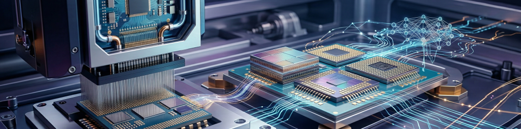
The semiconductor industry is undergoing a monumental architectural shift. Driven by the relentless demand for AI computing and high-performance computing (HPC), High Bandwidth Memory (HBM) and Chiplet-based designs have become the gold standard. However, this transition to 2.5D and 3D advanced packaging has triggered an unprecedented consequence: testing has rapidly become one of the most expensive and complex phases of semiconductor manufacturing.
As the value of a fully packaged AI accelerator reaches tens of thousands of dollars, the cost of a “bad die” escaping detection is catastrophic. Consequently, the industry is completely overhauling its approach to test engineering. In this comprehensive guide, we will analyze why HBM and Chiplet testing costs are surging, and how new strategies across Automated Test Equipment (ATE), advanced Probe Cards, Packaging Testing, Manufacturing Execution Systems (MES), and AI Quality Inspection are reshaping the manufacturing landscape.
1. The Root Cause: Why HBM and Chiplet Testing Costs Are Skyrocketing
To understand the cost surge, we must first examine the structural changes in modern semiconductor architectures. Legacy monolithic chips required straightforward wafer sort and final test protocols. Today’s heterogeneous integration completely changes the math.
1.1 The Known Good Die (KGD) Imperative
In a Chiplet architecture, multiple silicon dies (e.g., compute, I/O, memory) are integrated onto a single interposer or organic substrate. If just one of these dies is defective, the entire multi-chip package fails. The yield of the final package is the product of the yields of individual chiplets. Therefore, securing a 100% Known Good Die (KGD) before packaging is an absolute necessity. Achieving KGD requires exhaustive, at-speed testing at the wafer level, drastically driving up test times and costs.
1.2 The HBM Architecture Challenge
High Bandwidth Memory (HBM) involves stacking multiple DRAM dies vertically using Through-Silicon Vias (TSVs) and micro-bumps. Testing these vertical interconnects before, during, and after the stacking process is notoriously difficult. The sheer number of microscopic I/O connections means that traditional testing methodologies are no longer physically or economically viable.
2. Revolutionizing the Probe Card for High-Density Interconnects
The probe card is the critical physical interface between the ATE and the wafer. As bump pitches shrink to accommodate massive I/O densities, probe card technology is being pushed to its absolute limits.
2.1 The Micro-Bump Probing Dilemma
Advanced packaging relies on micro-bumps with pitches shrinking below 25 micrometers (μm). Traditional cantilever or standard vertical probe cards lack the precision to contact these microscopic bumps reliably without causing physical damage. Furthermore, standard probes cannot support the high-frequency signals required for HBM3 and HBM3e testing.
2.2 The Rise of Advanced MEMS Probe Cards
To solve this, the industry is rapidly transitioning to Micro-Electromechanical Systems (MEMS) probe cards.
- Precision and Density: MEMS manufacturing techniques allow for the creation of ultra-fine, highly dense probe arrays that perfectly match the micro-bump layout of Chiplets and HBM base dies.
- Signal Integrity: MEMS probes offer significantly shorter electrical paths, reducing parasitic inductance and capacitance, which is essential for preserving signal integrity during at-speed memory testing.
- Cost Implications: While MEMS probe cards are significantly more expensive to manufacture than traditional cards, their durability, precision, and ability to ensure KGD make them an indispensable investment for reducing overall packaging scrap rates.
3. Automated Test Equipment (ATE): Scaling for High Bandwidth and Thermal Loads
Automated Test Equipment (ATE) is the brain of the testing operation. Testing modern AI accelerators and HBM stacks requires ATE systems with unprecedented power, speed, and thermal management capabilities.
3.1 Managing Massive Parallel Testing
HBM architectures require simultaneous testing of thousands of I/O channels operating at gigabit-per-second (Gbps) speeds. Legacy ATE platforms do not have the pin count or the digital bandwidth to handle this. Next-generation ATE solutions are incorporating highly integrated digital instruments capable of driving and comparing massive parallel data streams, ensuring that the entire HBM stack functions synchronously.
3.2 The Thermal Management Crisis in ATE
Testing high-performance Chiplets and HBM at speed generates an immense amount of localized heat. If the die overheats during a test cycle, it can trigger thermal throttling, leading to false failures (yield loss) or, worse, physical damage to the silicon. Modern ATE setups must integrate advanced Active Thermal Control (ATC) systems. These handlers use liquid cooling and predictive thermal algorithms to dynamically inject or remove heat, maintaining the silicon at an exact temperature setpoint during high-power test vectors.
4. Next-Generation Packaging Testing: Final Test (FT) and System-Level Test (SLT)
Once the individual KGDs are packaged onto the interposer, the testing paradigm shifts. The complexity of 2.5D/3D interconnects mandates a multi-layered testing approach.
4.1 Structural and Functional Final Test (FT)
Final testing must ensure that the packaging process—such as the reflow of micro-bumps and the attachment to the interposer—did not introduce shorts or opens. Advanced Boundary Scan (IEEE 1149.1) and built-in self-test (BIST) methodologies are heavily relied upon to electrically verify internal TSVs and inter-die routing without requiring physical probe access.
4.2 The Shift Toward System-Level Test (SLT)
Because standard ATE functional testing cannot perfectly simulate the real-world operational environment of an AI data center, System-Level Testing (SLT) is becoming a mandatory step. SLT involves booting the packaged device using a real operating system and running actual application workloads (e.g., neural network inference tasks). While SLT adds significant cycle time and cost, it captures marginal defects—such as timing edge-cases between chiplets—that traditional ATE misses.
5. Software-Driven Yield: MES and AI Quality Inspection
Hardware alone cannot solve the testing cost crisis. Software intelligence is bridging the gap, turning massive streams of test data into actionable yield improvements.
5.1 Manufacturing Execution Systems (MES) as the Data Backbone
In a Chiplet ecosystem, components come from various foundries and fabs. A robust Manufacturing Execution System (MES) is critical for traceability. MES platforms track every single die from wafer sort through final packaging. By correlating SLT or ATE failure data back to specific wafer lots or probe card touches, MES enables root-cause analysis, allowing engineers to isolate parametric drifts and stop bleeding yield instantly.
5.2 AI Quality Inspection in Defect Detection
Visual and structural inspection of advanced packaging is no longer a task for human operators or basic rule-based computer vision.
- Automated Optical Inspection (AOI): AI-powered AOI systems utilize deep learning neural networks to inspect micro-bump coplanarity, TSV alignment, and underfill voiding.
- Predictive Maintenance: AI models analyze data from the ATE and probe cards in real-time to predict when a probe pin requires cleaning or replacement, thereby preventing cascading yield drops caused by degraded contact resistance.
6. Frequently Asked Questions: Navigating Advanced Semiconductor Testing
To assist engineering teams and procurement specialists, here are answers to the most common questions regarding HBM and Chiplet testing strategies.
Why is HBM testing significantly more expensive than standard DRAM?
HBM requires vertically stacking multiple DRAM dies using TSVs. Each layer must be thoroughly tested before and after stacking to ensure KGD. The extreme I/O density demands expensive MEMS probe cards and high-bandwidth ATE platforms, exponentially increasing both capital expenditure and test time.
What is the role of a probe card in Chiplet testing?
The probe card connects the ATE to the microscopic bumps on the silicon wafer. For Chiplets, it must precisely touch micro-bumps with pitches under 25μm to verify the die’s functionality before it is integrated into a multi-chip package, preventing expensive downstream scrap.
How does System-Level Test (SLT) differ from ATE?
ATE focuses on structural and deterministic functional testing using predefined vectors. SLT places the chip in its actual end-use environment, booting an OS and running real workloads to catch subtle timing or thermal marginalities that ATE might miss in highly complex Chiplet assemblies.
How is AI improving semiconductor packaging testing?
AI is primarily deployed in two ways: first, through advanced computer vision models for automated optical inspection (AOI) to detect microscopic packaging defects; second, through machine learning algorithms that analyze ATE data to predict equipment maintenance and identify systemic yield issues.
7. Conclusion: Strategic Investment in Test Capabilities
The narrative in semiconductor manufacturing has fundamentally changed. Testing is no longer an afterthought or a secondary cost center; it is the primary gatekeeper of profitability for advanced AI and HPC chips. As HBM and Chiplet architectures become standard, manufacturers must aggressively invest in next-generation ATE, ultra-precise MEMS probe cards, rigorous SLT protocols, and AI-driven MES platforms. Only by attacking the testing challenge holistically can the industry curb the surging costs and deliver the reliable computing power demanded by the AI revolution.
发表回复
要发表评论,您必须先登录。