MicroLED promises to outperform OLED in brightness, lifespan, and efficiency — yet mass production remains elusive. This deep dive examines the three interlocking bottlenecks holding MicroLED back, and explores how driver IC innovation, waveguide optics, and eye-tracking integration are shaping the display roadmap for consumer electronics and XR.
Why Is MicroLED So Hard to Mass-Produce?
MicroLED technology has been “just around the corner” for nearly a decade. The value proposition is compelling: self-emissive inorganic LEDs smaller than 50 µm delivering peak brightness exceeding 10,000 nits, effectively infinite contrast ratios, zero burn-in risk, and a color gamut that rivals or surpasses OLED — all without organic materials that degrade over time.
Yet in 2026, MicroLED displays remain confined to ultra-premium large-format signage, niche wearables, and pilot-line prototypes. Apple famously abandoned its in-house MicroLED effort, reverting to OLED. Samsung shelved its consumer MicroLED TV roadmap. AUO is ramping what Yole Group calls a “make-or-break” first production line.
The reason is a manufacturing triangle — three tightly coupled challenges that must be solved simultaneously:
- Mass transfer — moving millions of microscopic LED chiplets onto a backplane
- Driver IC and backplane design — electrically controlling each sub-pixel at extreme current densities
- Yield management — achieving defect rates low enough for consumer-grade displays
Solve any two without the third, and the economics collapse. This article unpacks each vertex of that triangle.
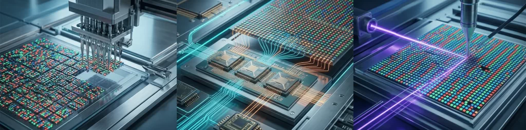
What Is Mass Transfer, and Why Is It the Central Bottleneck?
The Scale of the Problem
A 4K MicroLED display contains approximately 25 million sub-pixels (8.3 million RGB pixel groups × 3 sub-pixels). Each sub-pixel is an individual LED die that must be picked from a source wafer and placed onto a target backplane with sub-micron accuracy. For an 8K display, that number doubles to roughly 100 million.
Traditional LED packaging handles dies one at a time or in small batches. MicroLED demands massively parallel transfer — tens of thousands to millions of dies moved simultaneously — at throughputs compatible with display-panel production economics.
Competing Transfer Approaches
The industry has not converged on a single transfer method. Major approaches include:
- Stamp-based pick-and-place (PnP): An elastomeric stamp picks up an array of dies from a carrier wafer and prints them onto the backplane. Companies like X-Celeprint (acquired by TESORO Scientific) pioneered this approach. Throughput depends on stamp size and cycle time.
- Laser-assisted direct transfer (DTM): A laser selectively debonds MicroLEDs from a growth wafer directly onto a backplane with pre-patterned copper pads, enabling selective bonding and selective release. This eliminates the intermediate carrier step and is pursued by multiple research groups including CEA-Leti.
- Fluidic self-assembly: MicroLED dies are suspended in a liquid and guided into receptor wells on the backplane by shape-matching and capillary forces. eLux (now part of Lumens) explored this route.
- Electrostatic or electromagnetic transfer: Dies are manipulated using electric or magnetic fields for contactless placement.
Each method trades off throughput vs. placement accuracy vs. process complexity. As of early 2026, stamp-based and laser-assisted approaches lead in commercial readiness, but no single technique has achieved the combination of >99.999% placement yield and >50 million dies/hour throughput that consumer display economics demand.
Transfer Yield: The Numbers That Matter
Transfer yields today range from 3N (99.9%) to 5N+ (99.999%+) depending on die size and method. While 99.9% sounds impressive, for a 4K display with 25 million sub-pixels, a 99.9% yield means 25,000 defective pixels — clearly visible to the human eye. Even 99.99% (4N) leaves 2,500 defects.
The industry target is effectively 6N (99.9999%) or better, leaving fewer than 25 defects per 4K panel — manageable through pixel redundancy and individual pixel repair. Reaching this threshold at production-line throughput remains the defining challenge.
How Do Driver ICs and Backplane Design Constrain MicroLED Displays?
Why MicroLED Driving Is Fundamentally Different from OLED
OLED pixels are current-driven devices fabricated monolithically on a TFT (thin-film transistor) backplane. The organic emitter is deposited directly onto the backplane in a continuous process. The driver IC challenge is well-understood, and AMOLED pixel circuits using LTPS (low-temperature polysilicon) or LTPO TFTs are mature.
MicroLED inverts this paradigm. The emitter is a discrete inorganic die bonded to the backplane post-fabrication. This creates several unique driver IC and backplane challenges:
Ultra-High Current Density
MicroLED dies operate at significantly higher current densities than OLED sub-pixels of comparable size — particularly at small pixel pitches below 10 µm where efficiency droop and surface recombination become pronounced. The backplane must deliver stable, uniform current to millions of sub-pixels simultaneously without excessive voltage drop or thermal buildup.
Aperture Ratio and Interconnect Pitch
As pixel pitch shrinks, the available area for TFT circuitry and routing traces decreases dramatically. Achieving a high aperture ratio (the percentage of pixel area that actually emits light) while accommodating the bonding pads, driving transistors, and data/scan lines requires aggressive design-rule optimization — pushing LTPS backplanes toward their limits and driving interest in CMOS backplanes for micro-display applications.
CMOS vs. TFT Backplane Architectures
For large-format MicroLED displays (TVs, signage), LTPS-TFT backplanes remain the practical choice due to panel-size scalability. Imec, in collaboration with Barco, has developed alternative TFT pixel circuits that combine advantages of active-matrix and passive driving to optimize gray-level control, reduce flicker, and manage heat dissipation in modular MicroLED architectures.
For micro-displays targeting AR/VR headsets (pixel pitches of 3–5 µm), the industry is shifting to CMOS silicon backplanes where transistor density and switching speed far exceed TFT capabilities. CEA-Leti has championed a “CMOS-driven MicroLED” approach where the LED array is directly hybridized onto a silicon IC, enabling per-pixel PWM dimming, integrated test structures, and design-for-test (DFT) capabilities critical for yield management.
The Compensation Challenge
Unlike OLED, where pixel-circuit compensation corrects for organic material aging, MicroLED compensation must address LED-to-LED variation in forward voltage, wavelength, and luminous intensity arising from epitaxial non-uniformity and transfer-induced damage. This requires:
- Pre-transfer binning: Measuring and sorting dies on the source wafer before transfer
- Post-transfer calibration: Mapping the electrical and optical characteristics of every transferred die and writing per-pixel correction data into the driver IC
- In-field recalibration: Adjusting compensation tables over the product lifetime
The data volume is staggering: a 4K display needs per-pixel correction coefficients for current, voltage offset, and color — potentially hundreds of megabytes of calibration data per panel.
What Does the Yield Triangle Look Like in Practice?
Yield = Epitaxy × Transfer × Bonding × Test-and-Repair
The overall display yield is the product of yields at each process step. Current industry benchmarks:
| Process Step | Current Yield Range | Target for Consumer Displays |
|---|---|---|
| MicroLED chip (epitaxy + fab) | 99.0–99.5% | >99.9% |
| Mass transfer placement | 99.9–99.999% | >99.9999% |
| Electrical bonding | 99.5–99.9% | >99.99% |
| Post-transfer pixel functionality | 99.0–99.9% | >99.99% |
Compounding these yields for a 4K panel illustrates the problem. Even at the optimistic end of current ranges, the cumulative yield per sub-pixel is roughly 98–99%, leaving 250,000 to 500,000 potential defects per 8K panel. Without repair, this is commercially unacceptable.
Pixel Redundancy and Repair Strategies
The industry addresses residual defects through two complementary strategies:
- Redundancy: Fabricating spare sub-pixels at each pixel location. If the primary die is defective, the spare is activated. This trades panel area (lower aperture ratio) and driver complexity for higher effective yield.
- Individual pixel repair: Using laser-assisted techniques to remove a defective die and place a replacement. This is time-consuming and adds cost, but is necessary for panels where redundancy alone cannot achieve the target defect level.
Yole Group’s December 2025 analysis concluded that MicroLED must simultaneously achieve competitive die efficiency at small pixel sizes, mass-transfer yields above 5N, viable repair strategies, and overcome TFT-backplane limitations — all while matching OLED on cost. This is the “yield triangle” in its starkest form.
MicroLED vs. OLED: Where Does Each Technology Win?
Understanding MicroLED’s manufacturing struggles requires context on what it is competing against.
| Parameter | MicroLED | OLED |
|---|---|---|
| Peak brightness | >10,000 nits (potential) | 1,000–3,000 nits (current) |
| Contrast ratio | Infinite (self-emissive) | Infinite (self-emissive) |
| Burn-in risk | None (inorganic) | Moderate (organic degradation) |
| Lifespan | >100,000 hours | 30,000–50,000 hours typical |
| Color gamut | >100% DCI-P3 | ~99% DCI-P3 |
| Power efficiency | Higher (at scale) | Good, but blue degrades faster |
| Manufacturing maturity | Pilot / early production | Mature (Gen 8.5+ fabs) |
| Cost (55″ TV panel) | >10× OLED currently | Baseline |
OLED’s critical weakness — blue emitter lifetime — is being addressed by phosphorescent and TADF blue materials. If blue OLED lifespan improves significantly, MicroLED’s differentiators narrow to brightness and burn-in resistance, making the cost gap harder to justify for mainstream consumer products.
This competitive pressure is precisely why solving the mass-production triangle is urgent. MicroLED’s window of differentiation is not permanent.
How Are Waveguides and Eye Tracking Reshaping the MicroLED Opportunity in XR?
While large-format MicroLED displays struggle with cost, a different segment is emerging as a potentially faster path to volume: AR/XR micro-displays.
MicroLED Micro-Displays for AR Glasses
AR smart glasses require micro-displays with pixel pitches of 3–5 µm, extreme brightness (>100,000 nits at the emitter level to compensate for waveguide optical losses), and ultra-low power consumption. MicroLED is the only technology that can simultaneously deliver all three.
Companies like JBD (Jade Bird Display) and MICLEDI Microdisplays (an imec spin-off) are building MicroLED-on-CMOS micro-displays specifically for waveguide-based AR systems. These devices bypass the mass-transfer problem entirely for monochrome displays (the LEDs are fabricated directly on the CMOS wafer), though full-color versions still require color conversion or multi-chip integration.
The Waveguide Bottleneck
Waveguides — the thin, transparent optical elements that guide projected images from a micro-display to the wearer’s eye — are themselves a major manufacturing challenge. Current architectures include:
- Diffractive waveguides (used by Microsoft HoloLens, Meta Orion prototype)
- Holographic waveguides
- Geometric (reflective) waveguides
No single approach simultaneously solves all constraints: high optical efficiency, wide field of view, large eye-box, thin form factor, color uniformity, and manufacturability. Industry analysis suggests that breakthroughs in waveguide design — not GPU performance — will be the pacing factor for XR adoption.
For MicroLED, this means the micro-display must deliver enough raw brightness to overcome waveguide insertion losses (typically 90–99% of light is lost), making MicroLED’s inherent brightness advantage critical.
Eye Tracking: Enabling Foveated Rendering and Smarter Driving
Eye-tracking sensors integrated into XR headsets enable foveated rendering — rendering high resolution only where the user is looking, and lower resolution in the periphery. This has a direct impact on MicroLED driver IC design:
- Dynamic pixel addressing: The driver IC can modulate brightness and refresh rate per-region, reducing power consumption by 50–70% in theory.
- Reduced data bandwidth: Only the foveal region needs full-resolution data updates each frame.
- Adaptive brightness control: Eye-tracking data informs per-pixel dimming to optimize contrast and reduce visual fatigue.
This tight coupling between eye-tracking input and MicroLED driver output represents a systems-level co-design challenge that blurs the boundary between display hardware and computational optics.
What Is the Realistic MicroLED Commercialization Timeline?
| Timeframe | Segment | Status |
|---|---|---|
| 2025–2026 | Large-format signage / commercial | Limited production (AUO, Daktronics, Samsung) |
| 2025–2026 | AR/XR micro-displays | Pilot production (JBD, MICLEDI); dev kits shipping |
| 2026–2027 | Premium wearables / automotive HUD | Qualification and early adoption |
| 2027–2028 | Premium consumer TVs (>75″) | Dependent on transfer yield reaching 6N+ and cost reduction |
| 2029–2030+ | Mainstream consumer electronics | Requires cost parity with OLED; standardization of equipment |
Yole Group forecasts the MicroLED display market approaching $8 billion by 2032, but this is contingent on solving the yield triangle within the next 2–3 years.
Key Takeaways for Display and Semiconductor Engineers
- Mass transfer remains the gating bottleneck. No single transfer technology has achieved 6N yield at production-scale throughput. The industry urgently needs process standardization to reduce equipment cost and complexity.
- Driver IC design must co-evolve with the emitter. CMOS backplanes will dominate micro-displays for XR; LTPS-TFT backplanes must push aperture ratios and current handling for large-format panels. Per-pixel compensation data management is a non-trivial system design problem.
- Yield is a multiplicative chain. Epitaxy, transfer, bonding, and functional test yields all compound. Redundancy and repair are necessary but insufficient — each link must improve independently.
- OLED is not standing still. Blue phosphorescent and TADF emitter improvements are closing the lifespan gap. MicroLED must reach cost competitiveness before its differentiation window narrows.
- XR micro-displays may be the fastest path to volume. Monolithic MicroLED-on-CMOS architectures sidestep the mass-transfer problem for small-format displays, and waveguide-based AR glasses create a brightness-driven demand that only MicroLED can satisfy.
- Eye tracking transforms driver IC requirements. Foveated rendering integration demands dynamic, region-aware pixel driving — a systems-level challenge that rewards tight co-design between optics, sensors, and display silicon.
The MicroLED mass-production triangle — transfer, driver IC, yield — is not an unsolvable problem. It is an engineering and economic optimization problem that the display industry is attacking on multiple fronts. The question is whether solutions will converge fast enough to capture the market window before OLED closes the gap.
发表回复
要发表评论,您必须先登录。