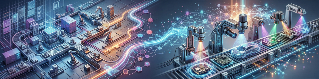
The landscape of electronics manufacturing is undergoing a profound paradigm shift. As we approach 2026, the integration of Artificial Intelligence (AI) at the manufacturing edge is accelerating at an unprecedented pace. For technical decision-makers, production managers, and test engineers, transitioning from traditional Manufacturing Execution Systems (MES) to AI-driven quality inspection is no longer optional—it is a critical requirement for survival. This 2026 roadmap explores the convergence of Automated Test Equipment (ATE), advanced probe cards, sophisticated packaging and testing workflows, next-generation MES, and AI quality inspection, providing a comprehensive guide to navigating the digitalized factory floor.
The Evolution of Test & Manufacturing: A 2026 Perspective
The demand for higher computational power, particularly driven by generative AI and advanced driver-assistance systems (ADAS), is pushing semiconductor nodes to their physical limits. Consequently, the test and manufacturing sectors must adapt to handle heterogeneous integration, chiplets, and 3D packaging.
Automated Test Equipment (ATE) Meets Artificial Intelligence
Automated Test Equipment (ATE) has traditionally relied on deterministic test vectors to validate System-on-Chip (SoC) functionality. However, as transistor counts exceed tens of billions per die, test times and data volumes have skyrocketed.
By 2026, AI-enhanced ATE is becoming the industry standard. Machine learning algorithms analyze historical test data to identify redundant test patterns, enabling adaptive testing. This means the ATE can dynamically adjust the test flow in real-time based on the early test results of a specific wafer batch, significantly reducing overall test time without compromising fault coverage. Furthermore, AI-driven ATE facilitates predictive maintenance, analyzing power consumption and signal integrity to flag potential hardware failures before they cause unexpected downtime.
Next-Generation Probe Cards for Advanced Packaging
Probe cards serve as the critical electromechanical interface between the ATE and the silicon wafer. With the rise of 2.5D and 3D packaging, pad pitches have shrunk drastically, demanding extreme precision.
In the 2026 roadmap, MEMS (Micro-Electro-Mechanical Systems) probe cards dominate the high-end market. These advanced probe cards offer superior signal integrity for high-frequency testing (such as PCIe Gen 5/6 and 800G optical transceivers). More importantly, digitalization integrates probe card lifecycle management directly into the MES. Edge AI monitors the contact resistance and physical degradation of probe needles in real-time, optimizing the cleaning recipe and extending the lifespan of these highly expensive consumables.
Transforming Packaging and Testing Workflows
Packaging and testing are no longer isolated backend processes. The shift toward advanced packaging requires a holistic, data-driven approach. Thermal dissipation, stress mismatch, and interconnect reliability are primary concerns when integrating multiple die into a single package.
Digitalized production lines utilize digital twins to simulate the packaging process. During actual production, inline metrology tools feed data continuously into the central control system. If an anomaly is detected during die attach or wire bonding, the system automatically adjusts parameters for subsequent steps, minimizing scrap rates and ensuring high yield in complex, high-margin products.
Bridging the Gap: How MES Integrates with AI Quality Inspection
The true power of the 2026 electronics manufacturing roadmap lies in the seamless integration of IT (Information Technology) and OT (Operational Technology). The bridge connecting these domains is the synergy between MES and AI Quality Inspection.
Traditional MES vs. AI-Enhanced MES
Traditional MES functioned primarily as a reactive system—tracking Work-in-Progress (WIP), managing inventory, and generating post-production reports. Data silos often prevented real-time decision-making.
The AI-enhanced MES of 2026 acts as the intelligent brain of the smart factory. It orchestrates the entire production flow by ingesting massive streams of time-series data from ATE, environmental sensors, and inline inspection tools. This modern MES leverages graph databases and machine learning to uncover hidden correlations—for example, linking a specific humidity variance during lithography to a localized yield drop detected during the final ATE test.
Deploying AI Quality Inspection on the Factory Floor
Traditional Automated Optical Inspection (AOI) and Automated X-ray Inspection (AXI) systems rely on rigid, rule-based algorithms. They frequently suffer from high false-call rates, requiring human operators to manually verify defects, which creates severe bottlenecks.
AI Quality Inspection revolutionizes this process using deep learning and computer vision.
- Defect Classification: Convolutional Neural Networks (CNNs) accurately classify defects (e.g., solder bridging, tombstoning, voiding) with human-level accuracy, drastically reducing false positives.
- Edge Inference: By deploying optimized AI models directly on edge devices via neural processing units (NPUs), inspection decisions are made in milliseconds, matching the high-speed cadence of surface-mount technology (SMT) lines.
- Continuous Learning: The AI systems are connected back to the MES. When a new defect anomaly occurs, the system flags it, human experts label it, and the model is retrained and redeployed seamlessly over-the-air (OTA).
Frequently Asked Questions (Voice Search & AEO Optimized)
What is the ROI of AI Quality Inspection in electronics manufacturing?
The Return on Investment (ROI) for AI Quality Inspection typically materializes within 6 to 12 months. Savings are driven by a 40-60% reduction in false-call rates, decreased manual labor costs, higher throughput, and the prevention of defective products reaching the market, thereby reducing warranty claims and protecting brand reputation.
How do smart probe cards improve ATE efficiency?
Smart probe cards improve ATE efficiency by utilizing embedded sensors to monitor contact resistance and mechanical wear in real-time. This data allows the MES to schedule predictive maintenance and optimize cleaning cycles, reducing unplanned ATE downtime by up to 30% and ensuring consistent signal integrity during high-speed wafer sorting.
What role does MES play in advanced packaging and testing?
In advanced packaging and testing, an AI-enhanced MES provides end-to-end traceability and real-time process control. It aggregates data across multiple disparate tools—from wafer dicing to final ATE testing—creating a unified digital thread. This allows manufacturers to correlate final test failures with specific upstream packaging parameters, enabling rapid root-cause analysis and yield optimization.
Conclusion: Embracing the Digitalized Factory
The journey from traditional MES to AI Quality Inspection represents a monumental leap in electronics manufacturing. By completely integrating ATE, next-generation probe cards, advanced packaging workflows, and deep learning-based inspection, factories in 2026 will achieve unprecedented levels of agility, yield, and efficiency. Manufacturers who proactively invest in this digital roadmap will secure a decisive competitive advantage in an increasingly complex semiconductor landscape.
发表回复
要发表评论,您必须先登录。