In the AI era, thermal management has become the single most critical constraint in semiconductor design. As chip power densities surge past 100 W/cm² in modern GPUs and AI accelerators, understanding exactly where heat is generated, how it flows, and where it gets stuck is no longer optional — it is the foundation of every reliable electronic product. The three-layer thermal resistance model — spanning die (chip), package, and system — provides the universal framework engineers use to decompose, quantify, and solve thermal challenges at every scale.
This article breaks down the three-layer model in detail, explains how thermal resistance is calculated and measured at each layer, and explores the real-world cooling technologies — cold plates, phase change materials (PCMs), heat pipes, and operational thermal monitoring — that map onto each layer of the stack.
Why the Three-Layer Model Matters in the Age of AI
Modern AI chips — NVIDIA’s GB200, AMD’s MI300X, Google’s TPU v5 — routinely dissipate 500 W to over 1,000 W per device. At these power levels, a 0.1 °C/W error in thermal resistance estimation can translate to a 50–100 °C miscalculation in junction temperature. That miscalculation can mean the difference between a chip that sustains peak performance and one that throttles within seconds.
The three-layer model decomposes the total thermal resistance from junction to ambient (θ_JA) into a series resistance chain:
θ_JA = θ_JC + θ_CS + θ_SA
Where:
- θ_JC (Junction-to-Case) = thermal resistance within the die and package, from the hottest transistor junction to the outer case surface.
- θ_CS (Case-to-Sink) = thermal resistance across the thermal interface material (TIM) between the package lid and the heat sink or cold plate.
- θ_SA (Sink-to-Ambient) = thermal resistance from the heat sink surface to the surrounding environment.
This decomposition is not merely academic. Texas Instruments’ widely referenced thermal metric application note describes a practical “three-resistor thermal approximation model” that uses θ_JC, θ_JB (junction-to-board), and an ambient convective resistance to estimate junction temperatures for any package on any board. The same conceptual framework scales from a 1 W microcontroller to a 1,000 W AI accelerator.
Layer 1: Die-Level Thermal Resistance (θ_JC)
What Happens Inside the Chip
Heat originates at the transistor junctions — billions of switching gates concentrated on a silicon die measuring just a few hundred square millimeters. In advanced nodes (3 nm, 5 nm), transistor density exceeds 100 million per mm², creating localized hotspots where power density can spike to 500–1,000 W/cm².
The thermal resistance from junction to case (θ_JC) captures the heat path through:
- The silicon die itself — Silicon has a thermal conductivity of ~150 W/m·K, which sounds high, but die thickness (50–775 µm) and non-uniform power maps create significant temperature gradients.
- Back-end-of-line (BEOL) metal layers — The interconnect stack above the transistors contains copper lines and low-k dielectrics. Low-k materials are thermally insulating (~0.2 W/m·K), creating a thermal barrier directly above the heat sources.
- Die-attach or TIM1 — The solder, adhesive, or thermal compound bonding the die to the package lid or heat spreader. This is often called TIM1 (Thermal Interface Material 1).
- Integrated heat spreader (IHS) or lid — Typically copper or nickel-plated copper, the IHS spreads concentrated die-level heat across a larger area before it exits the package.
How to Reduce θ_JC
- Die thinning: Reducing die thickness from 775 µm to 50–100 µm shortens the conduction path, directly lowering θ_JC. This is standard practice in 3D IC stacks.
- High-conductivity TIM1: Indium-based solders (thermal conductivity ~80 W/m·K) outperform thermal greases (~5 W/m·K) by an order of magnitude.
- Direct liquid cooling on die: TSMC and Microsoft have demonstrated microfluidic channels etched directly into silicon, bypassing TIM1 entirely and achieving thermal resistances below 0.01 °C/W.
3D IC Complexity
In chiplet-based and 3D-stacked architectures, the three-layer model must be extended. Each die-to-die interface adds a thermal resistance layer — microbumps (~50 µm pitch), underfill, and interposer materials all contribute. Research from IEEE shows that microbump thermal resistance in four-layer chip stacks can add 0.5–2.0 °C·mm²/W per interface, depending on bump pitch and underfill properties. Silicon interposers (~150 W/m·K) spread heat well, while organic interposers (~0.3 W/m·K) introduce significant thermal barriers.
Layer 2: Package-to-Sink Interface (θ_CS)
The Critical TIM2 Layer
Once heat exits the package through the IHS or lid, it must cross the interface to the heat sink or cold plate. This interface — filled by TIM2 — is often the largest single contributor to total thermal resistance in a well-designed system.
The interface thermal resistance depends on:
- TIM thermal conductivity (k): Ranges from ~1 W/m·K (basic thermal pads) to >50 W/m·K (metallic TIMs).
- Bond line thickness (BLT): Thinner is better. Typical BLT ranges from 25 µm (solder TIM) to 200 µm (gap pads).
- Contact resistance: Surface roughness and flatness of both the IHS and heat sink mating surfaces create microscopic air gaps that only a compliant TIM can fill.
The interface thermal resistance is approximated as:
θ_CS = BLT / (k × A) + R_contact
Where A is the contact area and R_contact accounts for surface imperfections.
What Are Phase Change Materials (PCMs)?
Phase change thermal interface materials are a class of TIM that transitions from solid to semi-liquid at a specific activation temperature (typically 45–60 °C). At operating temperature, the PCM softens and flows into every microscopic surface irregularity, dramatically reducing contact resistance.
Key advantages of PCMs for TIM2 applications:
- Ultra-low thermal resistance: Premium PCMs like Laird Tpcm™ 780 achieve bulk thermal conductivity of 5.5 W/m·K with minimal contact resistance, delivering total interface resistance below 0.05 °C·in²/W.
- No pump-out: Unlike thermal greases, PCMs do not migrate or dry out over time, maintaining consistent performance across thousands of thermal cycles.
- Clean application: PCMs ship as dry pads that can be pre-applied during manufacturing, simplifying assembly.
- Reworkability: The material can be cleanly removed for component replacement — critical for data center serviceability.
Honeywell, Parker Chomerics, and Laird all produce PCM-based TIMs specifically engineered for high-power semiconductor applications. For AI accelerators dissipating 500 W+ through a 50 × 50 mm lid, selecting the right TIM2 can mean a 10–15 °C difference in junction temperature.
How Do Cold Plates Reduce θ_CS and θ_SA?
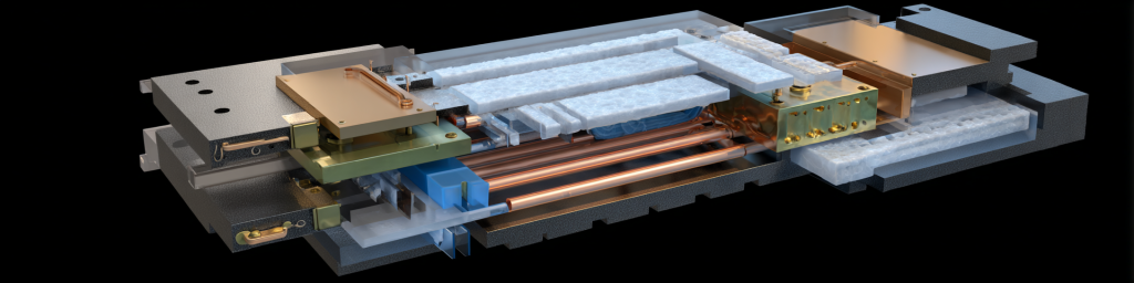
In direct-to-chip liquid cooling architectures, the cold plate replaces the traditional air-cooled heat sink entirely. A copper or aluminum cold plate with internal microchannels sits directly on the package lid (via TIM2), circulating coolant that absorbs heat at the source.
Cold plates effectively collapse θ_CS and θ_SA into a single, much lower thermal resistance. Water’s volumetric heat capacity is ~3,500× that of air, and forced convection through microchannels achieves heat transfer coefficients of ~15,000 W/m²·K — roughly 300× better than forced air.
A comprehensive review published in the journal Chemical Engineering Science (2025) documents cold plate technologies for data centers, covering microchannel geometries, coolant selection, and inlet/outlet optimization. The study confirms that well-designed cold plates achieve total thermal resistance (lid-to-coolant) of 0.02–0.05 °C/W for GPU-class devices — an order of magnitude lower than the best air-cooled heat sinks.
Advanced Cooling Technologies (ACT) recently demonstrated a two-phase cold plate dissipating over 7.5 kW from a single plate, simulating next-generation “superchip” thermal loads. Two-phase systems exploit the latent heat of vaporization, enabling even higher heat flux capacity than single-phase liquid cooling.
Layer 3: System-Level Thermal Resistance (θ_SA)
From Heat Sink to Ambient
The final layer captures how heat moves from the cooling device (heat sink, cold plate, or vapor chamber) to the ultimate heat sink — the surrounding air or a facility coolant loop.
For air-cooled systems, θ_SA depends on:
- Heat sink surface area and fin geometry — More surface area means lower resistance.
- Airflow velocity — Increasing airflow from 1 m/s to 3 m/s can halve θ_SA.
- Ambient temperature — A data center running at 35 °C ambient has less thermal headroom than one at 20 °C.
For liquid-cooled systems, θ_SA becomes the resistance of the broader coolant loop:
- Coolant flow rate and temperature — Higher flow and lower inlet temperature reduce resistance.
- CDU (Coolant Distribution Unit) capacity — The CDU rejects heat to facility water or an outdoor dry cooler.
- Facility-level rejection — Cooling towers, chillers, or dry coolers transfer data center waste heat to the outside environment.
The Role of Heat Pipes and Vapor Chambers
Heat pipes and vapor chambers are two-phase passive heat transport devices that dramatically improve heat spreading at the system level, reducing effective θ_SA.
How they work:
- A working fluid (typically water or a refrigerant) evaporates at the hot spot, absorbing latent heat.
- The vapor travels to the cooler condenser section at near-zero temperature gradient.
- The condensed liquid returns to the evaporator via capillary wicking in a sintered or grooved wick structure.
Heat pipes are tubular and excel at transporting heat over distances (10–300 mm) in one dimension. They are ubiquitous in laptop and desktop CPU coolers and are increasingly used in server heat sinks.
Vapor chambers are flat, plate-like heat pipes that spread heat in two dimensions. They are ideal for covering the large footprint of modern GPU packages. Boyd Corporation’s 3D vapor chamber assemblies are specifically designed for OCP Accelerator Module (OAM) form factors used in AI training servers.
A vapor chamber can reduce the temperature gradient across a 60 × 60 mm heat source from 15 °C (solid copper) to under 3 °C, effectively lowering the peak junction temperature by 12 °C or more.
Key comparison:
| Parameter | Heat Pipe | Vapor Chamber |
|---|---|---|
| Geometry | Tubular (1D transport) | Flat plate (2D spreading) |
| Typical thickness | 3–8 mm | 1–4 mm |
| Heat flux capacity | 50–200 W per pipe | 200–1,000+ W per chamber |
| Best for | CPU coolers, long-distance transport | GPU/AI accelerator base plates |
Operational Thermal Monitoring: Closing the Loop
Designing a low-thermal-resistance path is only half the battle. In production data centers, continuous thermal monitoring ensures the system operates within its thermal envelope over months and years of service.
Why Monitoring Matters
- TIM degradation: Thermal greases can pump out or dry out, increasing θ_CS by 50–100% over 2–3 years.
- Dust and airflow obstruction: Clogged filters or failed fans increase θ_SA unpredictably.
- Workload variation: AI training workloads can shift from 30% to 100% GPU utilization in seconds, causing rapid thermal transients.
- Ambient drift: Seasonal temperature changes and cooling system faults alter the operating point.
What to Monitor
- Junction temperature (T_J): Read directly from on-die thermal sensors via IPMI, Redfish, or vendor APIs. This is the ultimate metric — if T_J exceeds the thermal design point (typically 85–105 °C for modern GPUs), the chip throttles.
- Inlet and outlet coolant temperature: For liquid-cooled systems, the delta-T across the cold plate is a direct proxy for power dissipation and thermal resistance. A rising delta-T at constant power signals degradation.
- Ambient and rack-level temperature: ASHRAE recommends six sensors per rack (top, middle, bottom × front and back). Monitoring intake temperature ensures the cooling infrastructure delivers air or coolant within spec.
- Facility-level power and cooling metrics: PUE (Power Usage Effectiveness) tracks the ratio of total facility power to IT load power. A rising PUE signals cooling inefficiency.
Monitoring Technologies
- Embedded die sensors: All modern processors include multiple on-die temperature sensors with ±1 °C accuracy. Data is accessible via BMC (Baseboard Management Controller) interfaces.
- Wireless sensor networks: Companies like Monnit and RF Code provide battery-powered wireless sensors for rack-level environmental monitoring, feeding data into DCIM (Data Center Infrastructure Management) platforms.
- Infrared thermography: Non-contact IR cameras can detect surface temperature anomalies during maintenance windows — useful for identifying failed TIMs or blocked airflow paths.
- Continuous Thermal Monitoring (CTM): Exertherm and similar vendors provide permanently installed sensors on electrical distribution components (bus ducts, switchgear, PDUs), providing 24/7 early warning of thermal faults.
Predictive Maintenance
Advanced operators combine thermal telemetry with machine learning to predict failures before they cause downtime. By trending junction temperature, coolant delta-T, and fan RPM over time, anomaly detection algorithms can flag TIM degradation, pump failures, or coolant leaks weeks before they trigger thermal throttling.
Putting It All Together: A Practical Design Example
Consider a 700 W AI accelerator in a liquid-cooled server:
| Thermal Resistance Layer | Component | θ (°C/W) |
|---|---|---|
| θ_JC (die → lid) | Silicon die + indium TIM1 + copper IHS | 0.02 |
| θ_CS (lid → cold plate) | Phase change TIM2 (5.5 W/m·K, 50 µm BLT) | 0.01 |
| θ_SA (cold plate → coolant) | Microchannel copper cold plate, 25 °C inlet | 0.02 |
| Total θ_JA | 0.05 |
Junction temperature = T_coolant + (θ_JA × Power) = 25 + (0.05 × 700) = 60 °C — well within the 105 °C thermal limit, leaving ample headroom for workload spikes and aging.
If this same chip used air cooling with a traditional heat sink (θ_SA ≈ 0.10 °C/W, θ_CS ≈ 0.03 °C/W), total θ_JA would be ~0.15 °C/W, yielding T_J = 25 + 105 = 130 °C — far beyond safe operating limits. This arithmetic is precisely why liquid cooling has become non-negotiable for AI-class hardware.
Emerging Trends Shaping the Three-Layer Model
Direct-to-Silicon Microfluidics
Microsoft Research and TSMC are developing microfluidic channels etched directly into the back side of silicon dies. This approach eliminates TIM1 and the IHS entirely, collapsing θ_JC to near zero. Microsoft’s published results show cooling capacity improvements of up to 3× compared to conventional cold plates.
Two-Phase Immersion Cooling
Full immersion of servers in dielectric fluid eliminates the air-side thermal resistance entirely. While this changes the model (θ_SA becomes fluid-to-facility heat exchanger resistance), the three-layer decomposition still applies — the physics of series thermal resistance is universal.
AI-Driven Thermal Optimization
Neural Concept and other startups apply machine learning to optimize heat exchanger and cold plate geometries. By training on thousands of CFD simulations, AI models can generate designs that minimize thermal resistance while meeting manufacturing and pressure-drop constraints — compressing design cycles from weeks to hours.
FAQ: Common Questions About Thermal Resistance Modeling
What is the difference between θ_JA and Ψ_JT?
θ_JA (theta-JA) is the total thermal resistance from junction to ambient, measured under standardized conditions. Ψ_JT (psi-JT) is a thermal characterization parameter — not a true resistance — that relates junction temperature to the temperature measured at the top of the package. Ψ_JT is useful for in-situ monitoring but should not be used in the series resistance formula.
Can I simply add thermal resistances in series?
Yes, if the heat flow is predominantly one-dimensional and each layer sees the full power. In reality, heat spreading means some fraction of power flows through the board (θ_JB path). The three-resistor model is a practical simplification. For high-accuracy work, use finite-element thermal simulation tools like Ansys Icepak or Siemens Simcenter Flotherm.
How do I measure θ_JC in practice?
θ_JC is measured per JEDEC standard JESD51-14, using a cold plate with controlled surface temperature pressed against the package lid. By measuring junction temperature (via on-die diode) and case temperature (via thermocouple), θ_JC = (T_J − T_C) / Power.
What TIM should I use for AI accelerators?
For TIM1 (die-to-lid): indium solder or liquid metal for lowest resistance. For TIM2 (lid-to-cold plate): phase change materials (3–6 W/m·K) offer the best balance of performance, reliability, and serviceability. Metallic TIMs offer even lower resistance but complicate rework.
Conclusion
The three-layer thermal resistance model — θ_JC + θ_CS + θ_SA — remains the most powerful and practical framework for thermal design, from initial architecture through production monitoring. In the AI era, where every watt of cooling capacity translates directly to compute throughput and revenue, mastering this model is not just an engineering exercise — it is a competitive necessity.
By decomposing the thermal path into die-level, interface, and system-level resistances, engineers can pinpoint exactly where thermal bottlenecks exist, select the right technologies — phase change TIMs, liquid cold plates, heat pipes and vapor chambers, and continuous monitoring systems — and validate their designs with measurable, traceable metrics.
The chips will only get hotter. The engineers who understand where every fraction of a degree is won or lost will build the systems that keep AI running.
发表回复
要发表评论,您必须先登录。