The New Era of AI Processors: Beyond Transistor Scaling
The world of artificial intelligence processors is undergoing a fundamental shift. For decades, the primary driver of progress was making transistors smaller and cramming more onto a single piece of silicon, a trend known as Moore’s Law. Today, the explosive demands of AI infrastructure—powering everything from large language models to generative AI—are outpacing what traditional chip scaling can deliver alone.
The industry’s focus is pivoting from optimizing individual chips to a holistic, system-level design approach. This means engineers now design the computing cores, memory, connections, packaging, cooling, and power delivery as one cohesive unit from the start.
The Rise of Advanced Packaging and Chiplet Integration
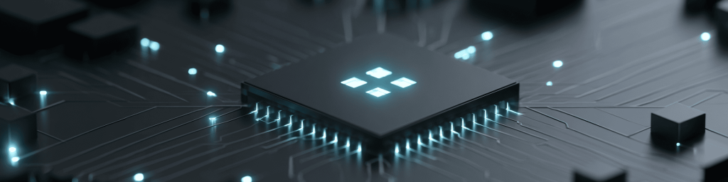
This transition is most evident in the rapid adoption of advanced packaging and chiplet-based designs. To break free from the physical and cost limitations of building everything on one large slab of silicon (a monolithic die), companies creating AI accelerators are turning to heterogeneous integration. Technologies like 2.5D and 3D Integrated Circuits (3DIC) allow different components to be built separately and then combined with incredible density. Alchip Technologies has become a pivotal player in this space, offering an advanced 3DIC platform specifically tailored for the massive scale of hyperscale AI and high-performance computing (HPC).
Why Monolithic Chips Struggle with Modern AI
The challenge for AI chip developers is no longer just about raw computing speed. Modern AI workloads require staggering amounts of memory bandwidth, ultra-low latency communication between components, and highly scalable connection architectures. Building a single, enormous processor chip is becoming economically and technically difficult. Physical limits on chip size and the plummeting manufacturing yields for large dies on cutting-edge process nodes make the monolithic approach increasingly impractical.
Chiplets: The Modular Answer
The semiconductor industry’s solution is the chiplet architecture. Instead of one giant processor, designers break down the functionality into multiple smaller, specialized dies. For example, the high-performance compute chiplets can be fabricated on the latest 3nm or 2nm technology for speed, while input/output (I/O) controllers and other functions can stay on older, more reliable and cost-effective nodes. These separate chiplets are then integrated into a single package using sophisticated interconnection technologies, creating a unified system.
Alchip’s 3DIC Platform: Building AI Subsystems
Alchip’s 3DIC platform embodies this architectural revolution. The company merges its custom chip (ASIC) design expertise with leading-edge packaging technologies from TSMC, such as CoWoS (Chip-on-Wafer-on-Substrate) and SoIC (System on Integrated Chips). The result isn’t just a chip; it’s a scalable AI processor subsystem. A typical powerful AI accelerator package enabled by Alchip might contain several compute chiplets, stacks of High Bandwidth Memory (HBM), and dedicated I/O dies—all working together in a package that can handle power levels measured in kilowatts.
Solving the Memory Bottleneck with 2.5D/3D Packaging
A key driver for this system-level integration is memory bandwidth, a major bottleneck in AI computing. AI accelerators need to move vast amounts of data to and from high-bandwidth memory (HBM) at incredible speeds. Old packaging methods simply can’t provide the dense, energy-efficient connections required. Advanced 2.5D and 3D packaging architectures solve this by placing dies much closer together, enabling thousands of ultra-short, parallel connections that drastically boost speed and efficiency.
Packaging is as Strategic as Transistor Technology
Industry experts now see advanced packaging technology as being just as strategically vital as transistor scaling itself. TSMC’s CoWoS packaging, for instance, is at the heart of nearly every top-tier AI accelerator today, creating huge demand. Alchip’s deep knowledge in CoWoS integration and managing the complex manufacturing flow places it at the center of one of the AI semiconductor sector’s fastest-growing areas.
Managing Unprecedented Heat in AI Systems
Another critical trend is thermal management. As more computing power and memory stacks are packed into a single package, power densities reach new heights. Dissipating this heat becomes a primary design constraint, requiring a co-design effort that considers the silicon, the package, the substrate, and the cooling solution simultaneously.
Alchip’s 2nm Platform and Heterogeneous Integration
Alchip’s work on a 2nm platform showcases the future of AI processors. This platform allows for the combination of 2nm compute dies with 3nm or 5nm I/O chiplets, using various advanced packaging options like CoWoS-L and SoIC stacking. This highlights a widespread industry understanding: the best AI systems won’t use just one manufacturing process. Instead, they will be smart assemblies of specialized dies, each made on the most optimal technology node for its function.
The Role of Standards: UCIe and Optical Interconnects
UCIe: Enabling a Chiplet Ecosystem
The development of the UCIe (Universal Chiplet Interconnect Express) standard is accelerating the move to modular AI systems. This standardized connection protocol allows chiplets from different suppliers to communicate efficiently, fostering a more flexible and innovative ecosystem. Other companies are already demonstrating high-speed UCIe implementations for advanced AI packages.
The Optical Frontier: Co-Packaged Optics
Looking beyond electrical connections, the next breakthrough may be in light. Alchip has partnered with Ayar Labs to develop co-packaged optical solutions for massive, rack-scale AI clusters. These designs integrate tiny light-based communication engines right inside the AI processor package. This promises ultra-high bandwidth connections between processors with far lower latency and energy use than electrical wires, which will be crucial as AI models scale across thousands of chips.
The Bottom Line: A New Competitive Landscape
The broader takeaway is that competition in AI semiconductors is evolving. Leading the race is no longer just about who has the best transistor technology. Success increasingly depends on mastering system integration, advanced packaging, software, memory architecture, and power efficiency all at once. The AI “processor” is transforming from a standalone chip into a complete, tightly integrated computing platform.
Alchip’s 3DIC strategy is a clear example of this transformation. By focusing not just on transistor performance but on enabling modular, heterogeneous, and scalable AI infrastructure architectures, Alchip is aligning with the future of the semiconductor industry: an era of system-level engineering where the package, the interconnects, and the overall architecture are as critical as the processor core itself.
发表回复
要发表评论,您必须先登录。