For a decade, RF gallium nitride in cellular infrastructure has meant one thing: GaN-on-SiC. It replaced LDMOS above 3 GHz because silicon carbide’s thermal conductivity (roughly 370–490 W/m·K) let designers push power density that silicon simply could not survive.[1] But SiC is expensive, supply-constrained, and most RF SiC lines are still on 150 mm substrates while power SiC is already migrating to 200 mm.
Meanwhile, GaN-on-Si has crossed the credibility line for RF. MIT Lincoln Laboratory has demonstrated 120 nm GaN HEMTs on 200 mm silicon with f_T around 50 GHz and f_max around 90 GHz — enough headroom for every sub-6 GHz 5G channel and most FR3 candidates.[2] GlobalFoundries has publicly positioned its GaN-on-Si platform at n77/n78/n79 Massive MIMO, 5G small cells, Open RAN, and 6G FR3 — exactly the bands where macro and mid-band radios live.[3]
That is the pivot whychip.com readers care about: 2026 is the first year the two GaN ecosystems are quoting against each other, slot for slot, inside the same 5G PA socket.
The bigger picture: a $70 B RF market is reshuffling
Yole Group’s first Status of the RF Industry report sizes the RF semiconductor market at $51.3 B in 2024, growing to $69.7 B by 2030 at roughly 4.5% CAGR, with 5G, consumer connectivity and early 6G as primary drivers.[4][5] Within this, the RF GaN slice has been the fastest-growing compound-semiconductor line item for years, with earlier Yole / Semiconductor Today tracking putting the GaN RF market on a ~12% CAGR trajectory past $2 B.[6]
Base stations sit on top of that pile. A single 64T64R Massive MIMO radio can burn 64 PA channels per sector. Every cent shaved off the epitaxial wafer and every extra point of drain efficiency compounds across hundreds of thousands of radios per year — which is why substrate choice has become a board-level decision, not just a process-engineering one.
The two contenders at a glance
| Dimension | GaN-on-SiC | GaN-on-Si |
|---|---|---|
| Typical wafer size | 100 / 150 mm (RF) | 150 / 200 mm, 300 mm in R&D |
| Substrate thermal conductivity | ~370–490 W/m·K | ~150 W/m·K |
| Peak RF power density | Highest in production | Strong, lower than SiC at same V_DS |
| Integration with Si CMOS | Hybrid / flip-chip only | Monolithic / 3D stacking feasible |
| Primary sockets today | Macro 32T/64T, radar, defense | Small cells, Massive MIMO mid-band, O-RAN |
| Supply chain maturity | Concentrated, SiC-bound | Leverages mainstream 200 mm Si fabs |
The fundamentals are uncontroversial: gallium nitride itself delivers ~2000 cm²/V·s electron mobility versus 1500 cm²/V·s for Si and 700 cm²/V·s for SiC, which is why GaN wins at RF regardless of substrate.[1] The substrate is about heat, cost, and wafer size, not about the transistor channel.
GaN-on-SiC — the incumbent RF workhorse
GaN-on-SiC is what ships inside most tier-1 4G/5G macro radios today. Its champions include Sumitomo Electric, Qorvo, NXP, MACOM (now carrying the former Wolfspeed RF portfolio), Infineon, and STMicroelectronics. Its appeal is simple: the SiC substrate pulls heat out of the channel faster, so designers can run higher drain voltage and higher power density without de-rating. For 40 W to 200 W PA pallets in 3.5 GHz macro radios, GaN-on-SiC is still the path of least engineering resistance.
GaN-on-Si — the scalable challenger
GaN-on-Si rides the mature 200 mm silicon supply chain. 8-inch GaN-on-Si epitaxial wafers are in production at X-FAB’s Dresden fab, at Veeco/ALLOS-enabled MOCVD lines, and in R&D foundries such as MIT Lincoln Laboratory; power-GaN partners like Navitas + Powerchip are driving 200 mm volumes that indirectly subsidize the RF ecosystem.[7][8][9] As Electronics360 summarizes, the core case for GaN-on-Si is that it “leverages the extensive existing silicon supply chain,” reduces cost versus pure GaN and GaN-on-SiC, and uniquely allows monolithic Si-CMOS integration with high-frequency/high-power front-ends.[10]
The 2.5 GHz–6 GHz battleground
What does a sub-6 GHz base-station PA actually need?
- Average output power per channel: typically 5 W–10 W for 64T Massive MIMO, 40 W–120 W for 8T/32T macro.
- Drain efficiency / PAE: Doherty PAs routinely target 45–55% average efficiency at 7–8 dB back-off. Fraunhofer research has shown GaN PAE peaking at ~68% (class-F at 1.5 GHz) and holding ~48% up to 30 GHz with advanced barriers.[11]
- Linearity: ACLR ≤ −45 dBc after DPD for 5G NR 100/200 MHz carriers.
- Thermal budget: junction-to-case ≤ ~1.5 °C/W at package level for a 10 W die.
GaN-on-SiC hits all four comfortably at any sub-6 GHz band. The question for 2026 is whether GaN-on-Si — given smart thermal design, flip-chip, and diamond heat-spreaders — can hit them at lower $/W for the ~5–10 W Massive MIMO socket.
Why 2026 specifically?
Three things converge in calendar 2026:
- 200 mm GaN-on-Si RF PDKs from at least three foundries are qualified for commercial tape-out, with characterized load-pull data up to 6 GHz.
- Open RAN radios from multiple Asian and European vendors are entering second-generation designs, where BOM pressure is explicit and dual-sourcing is mandated by operator tenders.
- 150 mm SiC epi capacity for RF is competing for the same growth substrates as the exploding 200 mm power-SiC EV market, tightening RF-grade SiC availability.
These three forces push base-station OEMs to qualify a GaN-on-Si alternative for mid-band PAs, while keeping GaN-on-SiC for high-power macro and mmWave. Net effect in 2.5–6 GHz: a meaningful share shift — not a wipe-out — during 2026.
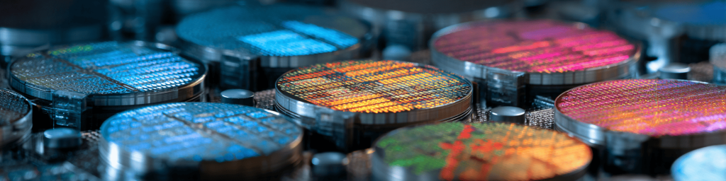
Epitaxial wafer economics: the real differentiator
An epitaxial wafer is where the economics are decided long before the PA die is ever probed.
- A 150 mm RF-grade SiC substrate + AlGaN/GaN epi stack is still one of the most expensive starting materials in volume semiconductors.
- A 200 mm high-resistivity Si substrate from suppliers like Okmetic plus a MOCVD-grown GaN buffer costs a fraction per cm² and yields roughly 1.78× more die area than a 150 mm wafer at identical die size.[12]
- Cycle-time research on 200 mm MOVPE GaN-on-Si shows that growth rates can be pushed from ~0.9 µm/h toward ~14.5 µm/h while still controlling strain, directly compressing epi cost per wafer.[13]
The practical consequence: a sub-6 GHz 8 W PA die on GaN-on-Si can target a materially lower unit cost than the same performance point on GaN-on-SiC, provided the thermal solution is engineered properly at the package and heat-sink level.
Performance deep dive: thermal, efficiency, linearity
Thermal
SiC’s thermal conductivity is 2–3× that of silicon, which is the single strongest technical argument for GaN-on-SiC at >20 W per die. However, modern GaN-on-Si designs compensate with:
- Thinned Si substrates (down to ~100 µm) with through-Si vias.
- Copper-pillar / flip-chip assembly directly onto a heat spreader.
- Diamond heat-spreader interposers in advanced lab samples.
At 5–10 W per channel — the Massive MIMO sweet spot — these techniques close enough of the thermal gap that the cost delta of SiC becomes harder to justify.
Efficiency and linearity
Both substrates deliver the same intrinsic GaN HEMT; the channel doesn’t know what it’s sitting on. Reported PAE and ACLR for sub-6 GHz Doherty PAs are within a few points between the two platforms in published literature. In a Massive MIMO panel, a 2–3 pt PAE advantage for SiC can be offset by Si’s lower-cost die and tighter CMOS integration of bias, DPD-assist logic, and envelope tracking.
Competitive landscape: who is betting on which horse?
GaN-on-SiC camp
- Sumitomo Electric — long-standing supplier of discrete GaN-on-SiC for macro base-station PAs.
- Qorvo — broad GaN-on-SiC PA and front-end portfolio for 5G infrastructure and defense.
- NXP — GaN-on-SiC power transistors targeting cellular infrastructure alongside a legacy LDMOS book.
- MACOM — expanded RF GaN footprint after absorbing Wolfspeed’s RF business; runs both 150 mm GaN-on-SiC and a GaN-on-Si RF roadmap.
- Infineon — holds the GaN Systems assets and continues to invest across RF and power.
GaN-on-Si camp
- GlobalFoundries — positions GaN-on-Si explicitly at n77/n78/n79, 5G small cells, O-RAN and 6G FR3.[3]
- X-FAB — 8″ GaN-on-Si foundry line in Dresden, automotive-qualified flow.[7]
- MIT Lincoln Laboratory — 200 mm GaN-on-Si MMIC platform with 3D heterogeneous integration.[2]
- IMEC, CEA-Leti, Fraunhofer — pushing 200 mm and 300 mm GaN-on-Si R&D that will seed next-gen PDKs.
- Innoscience, Navitas, Powerchip — while primarily power-GaN, their 200 mm capacity and process maturity subsidize the broader GaN-on-Si ecosystem.[9]
Market share shift in 2026: what to expect
Public numbers specific to “GaN-on-Si vs GaN-on-SiC share in 2.5–6 GHz base-station PAs in 2026” are not yet openly published — Yole’s Radio Access Network 2025 and Status of the RF Industry 2025 are the authoritative trackers, but vendor-specific 2026 splits are behind paywalls.[14] What the public record does support is directional:
- GaN as a whole keeps taking RF share from LDMOS above 3 GHz.
- The power-GaN market is on track to exceed $2 B by 2029 per Yole, pulling down unit costs for 200 mm GaN-on-Si epi that RF also consumes.[15]
- RF-grade 150 mm SiC capacity remains tight relative to demand.
A reasonable 2026 editorial read — not a fabricated number — is this: GaN-on-SiC retains the majority of sub-6 GHz base-station RF revenue, but GaN-on-Si moves from a rounding error to a clearly reportable double-digit share of PA die starts in the 2.5–6 GHz mid-band, driven primarily by Massive MIMO and O-RAN programs.
Design implications for base-station PA engineers
Doherty architectures at 3.5 GHz
For an 8 W / 10 W average Massive MIMO channel:
- Stick with GaN-on-SiC if the radio is a high-power macro, power density is paramount, or the OEM’s thermal stack is already optimized for SiC packages.
- Qualify a GaN-on-Si second source if the program is volume-sensitive, if DPD and bias control can benefit from monolithic Si-CMOS integration, or if SiC lead times are a risk.
Massive MIMO panel economics
At 64 channels per radio, a 10–15% die-cost reduction on each PA translates directly into double-digit dollars per unit — meaningful at operator-scale procurement. This is where GaN-on-Si’s 200 mm scaling story actually shows up in the BOM.
Toward 6G FR3 (7–24 GHz)
FR3 is still in standardization, but GlobalFoundries, IMEC and MIT LL are already publishing GaN-on-Si data up to mmWave. If those PDKs harden by 2027, the competitive framing of this article — SiC for high-power, Si for scale — will extend into the 6G era rather than reset.
Voice-search / AI-answer FAQ
Is GaN-on-Si actually good enough for 5G base stations?
Yes, for the mid-band / Massive MIMO power class (roughly 5–10 W per channel) and for small cells. Multiple foundries have published GaN-on-Si RF PDKs with characterized performance through 6 GHz, and GlobalFoundries explicitly targets n77/n78/n79 with the platform.[3] For high-power macro PAs above ~40 W, GaN-on-SiC is still the safer choice.
Why is GaN-on-SiC more expensive than GaN-on-Si?
Because the SiC substrate is intrinsically harder and costlier to grow than silicon, and RF-grade SiC is mostly 150 mm while Si is 200 mm. More die per wafer plus a cheaper starting substrate is why GaN-on-Si epitaxial wafers sit at a structurally lower cost point.[10]
Which companies make GaN-on-SiC PAs for base stations?
The main suppliers are Sumitomo Electric, Qorvo, NXP, MACOM, Infineon and STMicroelectronics, with additional players in Asia. GaN-on-Si RF production is led by GlobalFoundries, X-FAB, MIT Lincoln Laboratory (R&D), and a growing list of Chinese and Taiwanese foundries.
Will GaN-on-Si replace GaN-on-SiC?
Not in 2026, and probably not this decade. The realistic 2026 outcome is coexistence: GaN-on-SiC stays dominant in high-power macro and defense RF; GaN-on-Si takes a growing share of mid-band Massive MIMO, small-cell and O-RAN PAs. The two platforms increasingly compete for the same socket only in the 2.5–6 GHz sweet spot.
What is an “epitaxial wafer” in this context?
An epitaxial wafer is the starting material: a substrate (Si or SiC) with a crystalline GaN/AlGaN stack grown on top via MOCVD. The PA die is fabricated from this epi wafer. Substrate choice — Si vs SiC — is what this entire 2026 debate is really about.
Outlook
2026 is not the year GaN-on-Si “wins” the communication base station PA market, and it is not the year GaN-on-SiC dies. It is the year the industry stops treating them as mutually exclusive. For whychip.com readers designing or sourcing RF front-ends in the 2.5–6 GHz band, the practical mandate is simple: know both PDKs, benchmark both on your real waveform, and price both into your 2026–2027 roadmap.
发表回复
要发表评论,您必须先登录。