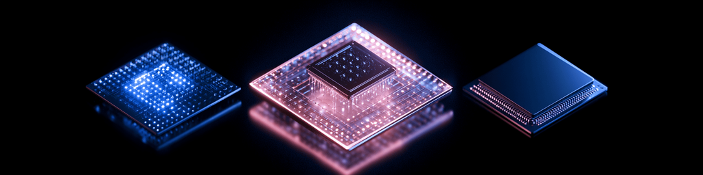
Intel EMIB and Intel Foveros are two cutting-edge semiconductor packaging solutions built to combine multiple silicon dies (also called chiplets) into a single processor package. Both support chiplet integration (heterogeneous integration): manufacturers can build different functional components using the process technology best suited for each, then link them to work as one unified system. Their core difference is in chiplet arrangement: EMIB connects dies placed side-by-side, while Foveros enables vertical die stacking.
What is Intel EMIB Technology?
EMIB stands for Embedded Multi-die Interconnect Bridge. Instead of placing all chiplets on a large, costly silicon interposer, Intel embeds tiny silicon bridges directly into the package substrate. The edges of adjacent dies sit right above these bridges, communicating through dense microscopic connections. Since silicon bridges are only placed where high-bandwidth links are required, EMIB avoids the high cost and manufacturing complexity of a full-size interposer, while still delivering far denser data transfer than standard circuit board connections.
Benefits and Limitations of EMIB
This side-by-side layout makes EMIB ideal for connecting large logic dies, accelerator tiles, input/output chiplets and high-bandwidth memory. Every component has direct access to the package surface, which simplifies power delivery and cooling. The architecture also works with dies of different sizes and produced on different process nodes. Its main downside is spatial: adding more chiplets widens the package, which can increase its total footprint and the distance between some components.
What is Intel Foveros Vertical Packaging?
Foveros takes a vertical approach to 3D IC packaging. In a standard Foveros design, one or more compute dies are mounted on top of a base die. Fine-pitch connections carry data and power between the layers, so the stacked dies function as a tightly integrated system. The base die can be active silicon with communication, input/output or power management circuits, not just a passive mounting surface. This creates a solution close to a full three-dimensional system on a package.
Advantages of Foveros Stacking
Vertical stacking brings multiple benefits. It shortens connections between functional blocks, boosts interconnect density, and fits more computing power into a smaller footprint. Designers can split processor functions that used to occupy one large monolithic die. For example, high-performance CPU or graphics tiles can be fabricated on an advanced cutting-edge process, while less performance-critical input/output functions use a cheaper, more economical process. Smaller dies also often have better manufacturing yields than one huge single piece of silicon.
Key Challenges for Foveros Implementations
Foveros comes with challenges that are far less severe with side-by-side EMIB designs. Heat produced by a lower die has to pass through the material above it, and an upper die can block cooling for the base layer. Delivering power through the stack and testing individual components also requires careful engineering work. Manufacturing tolerances get much stricter as connection pitches shrink. Intel’s Foveros Direct solves interconnect performance issues by using copper-to-copper hybrid bonding, which creates dense, low-resistance links without needing traditional solder bumps.
Which Technology Fits Your Design Needs?
The two technologies are built for different design requirements. EMIB is a great choice when you have several large dies or memory stacks that need high-bandwidth lateral connections, simple cooling, and a cost-effective alternative to a large interposer. Foveros is the better pick when package space is limited, or you need extremely dense links between logically connected layers. EMIB builds outward, while Foveros builds upward. Neither technology is universally superior, because bandwidth, power, cooling, yield, package size and manufacturing cost must be balanced for every individual product.
Complementary Use in 3.5D Packaging
Most importantly, EMIB and Foveros are complementary rather than mutually exclusive. Intel can combine the two in what it calls 3.5D packaging. Foveros creates individual vertical stacks, while EMIB bridges connect those stacks to other compute tiles or high-bandwidth memory placed next to them. This lets designers build complex processors from specialized building blocks, instead of having to fit every function onto a single large die.
Final Takeaway
To sum it up: EMIB links adjacent chiplets using small, localized silicon bridges embedded in the package, while Foveros stacks dies and connects them vertically. EMIB focuses on flexible lateral integration, easy cooling and efficient connections between large components. Foveros focuses on compact size, short communication paths and three-dimensional integration. Together, they show that advanced packaging is now just as important as transistor scaling: future performance gains will rely not just on making transistors smaller, but also on arranging specialized silicon components and moving data between them efficiently.
发表回复
要发表评论,您必须先登录。