When the Snapdragon 8 Elite Gen 5, MediaTek Dimensity 9400+, Apple’s A19 Pro-class silicon, and Samsung’s first 2 nm Exynos-class mobile processors sit idle, they behave like any other chip. The moment a user fires up a large language model (LLM), on-device Stable Diffusion, real-time translation, or a generative camera pipeline, the entire neural-processing subsystem lights up — and a 6.5-inch slab of glass, metal, and battery suddenly has to dissipate a sustained power envelope that looks more like a thin-and-light laptop than a phone. Industry analysts and thermal engineers have been consistent on one point: by late 2025, vapor chambers had become standard in top-tier phones and laptops specifically to reduce throttling, and that trend is accelerating in 2026 with larger chambers and better heat spreading.[1]
But a vapor chamber is only as good as the thermal interface material (TIM) between it and the SoC die. If that 50–100 µm layer cannot move heat fast enough, the rest of the thermal stack — graphite sheets, mid-frame, back cover — sits starved of energy to dissipate. This is why nano-scale TIMs have quietly become one of the most strategically important passive components in the AI smartphone supply chain.
“Thermal interface materials fill micro- and nano-scale gaps between chips and heat sinks to promote interfacial heat transfer and lower contact thermal resistance, thereby improving overall heat dissipation efficiency.” — ScienceDirect, 2026 review on low-thermal-resistance TIM design[2]
What Is a Nano-Scale TIM, Exactly?
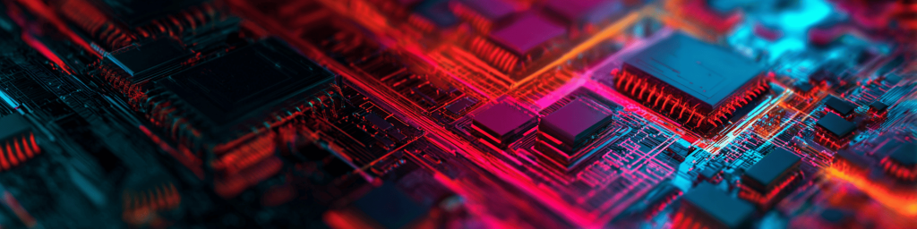
A TIM is the soft, compliant layer that sits between a heat source (the SoC die or its integrated heat spreader) and a heat sink (vapor chamber, graphite sheet, or mid-frame). Without a TIM, two “flat” metal surfaces only touch at a handful of microscopic asperities; more than 99% of the nominal contact area is actually air, which is a near-perfect thermal insulator (~0.026 W/m·K).
A nano-scale TIM goes a step further than traditional silicone greases: it uses nanostructured fillers — graphene nanoplatelets, vertically aligned carbon nanotubes, boron nitride nanosheets, or liquid metal nano-droplets — to build a continuous phonon-conduction network through an otherwise insulating polymer matrix, while keeping the bond-line thickness (BLT) well under 100 µm.
How a TIM Is Actually Measured
Engineers rarely care about a single headline number. The four metrics that matter for an AI phone TIM are:
- Bulk thermal conductivity (k) in W/m·K — in-plane and through-plane are usually different.
- Bond-line thickness (BLT) in µm — thinner is almost always better.
- Contact thermal resistance (Rc) in cm²·K/W — the real figure of merit at the interface.
- Long-term stability — pump-out, dry-out, oxidation, and mechanical cycling under thousands of thermal shocks.
The 2026 Inflection Point: Why On-Device AI Broke the Old TIM Playbook
For roughly a decade, the mobile industry relied on silicone greases loaded with alumina or zinc oxide, delivering 3–6 W/m·K. That was perfectly adequate when the SoC spent most of its day sipping a few hundred milliwatts. AI workloads changed the duty cycle.
- Sustained NPU load, not peak CPU load, is the new thermal villain. An LLM answering a long prompt can hold the NPU and memory subsystem at a high fraction of TDP for tens of seconds — far longer than a camera burst or a game frame.
- 2 nm and N3P-class nodes concentrate heat into smaller dies. TSMC’s advanced lithography has pushed smartphone SoCs toward ~5 GHz peak clocks,[3] and MediaTek has publicly committed to a first-of-its-kind SoC on TSMC’s N2P process.[4] Smaller dies mean higher heat flux (W/cm²) even when total power stays flat.
- 3D stacking and advanced packaging — the same trends driving AI accelerators — are beginning to reach mobile, trapping heat under upper dies that the TIM must still evacuate.[5]
The net effect: the last 100 microns between die and vapor chamber now dominate the end-to-end thermal budget. That is exactly where nano materials earn their place.
The Nano-Material Toolbox for AI Smartphone TIMs
1. Graphene-Based TIMs — The Current Champion in Mobile
Graphene’s intrinsic in-plane thermal conductivity is famously high — commonly reported in the 3,000–5,000 W/m·K range for high-quality single layers.[6][7] In practice, composites and films deliver a fraction of that, but still vastly outperform legacy pastes:
- Commercial graphene TIM pads now report in-plane conductivity up to ~600 W/m·K and through-plane (Z-axis) values of 70–130 W/m·K.[8]
- A 2026 IEEE EPS paper on graphene-enhanced TIMs documents through-plane thermal conductivity up to ~100 W/m·K using vertically oriented graphene architectures.[9]
- Recent academic work combines magnetic-field-assisted alignment with catalytic graphitization to reduce phonon scattering and push graphene-film conductivity further.[10] A March 2026 Applied Physics Letters paper introduces “Baumkuchen”-inspired architectures aimed at high through-plane conductivity for TIMs.[11]
Crucially, early 2026 brought clearer industry testing standards for graphene, which lets OEMs compare suppliers on an apples-to-apples basis for the first time.[1] That alone is unblocking graphene adoption in flagship phones.
2. Carbon Nanotube (CNT) TIMs — High-Performance, Still Scaling
Vertically aligned CNT (VACNT) forests behave like dense fields of tiny thermal “bristles” that compress between die and heat spreader, giving very low contact resistance at ultra-thin BLTs. IDTechEx’s thermal management reports highlight VACNT as a serious TIM candidate, while also flagging the central manufacturing challenges: transferring aligned arrays to real substrates and scaling yield.[12] Companies such as Carbice are actively commercializing CNT-based thermal interfaces, partnering with Dow Silicones on next-generation formulations.[13]
For AI phones specifically, CNT TIMs are attractive because they tolerate repeated mechanical cycling (pocket flex, drops, hinge compression on foldables) without the pump-out behavior that plagues greases.
3. Liquid Metal TIMs — Unmatched k, But a Packaging Problem
Liquid metal alloys (typically gallium-based eutectics) can exceed 30 W/m·K as bulk TIMs,[14] and peer-reviewed work shows sandwich-style LM/indium/LM pads achieving thermal resistance as low as 0.036 cm²·K/W on a real commercial smartphone test vehicle.[15] Xiaomi, ROG, and other gaming-phone OEMs have shipped liquid-metal-based interfaces in limited volumes, and Apple is widely reported to be exploring Liquidmetal-class amorphous alloys for its foldable iPhone hinge in 2026.[16][17]
The drawback: gallium alloys are electrically conductive and chemically aggressive toward aluminum. In a phone, a single droplet migrating onto a PCB trace is catastrophic. That is why encapsulated liquid-metal composites — liquid metal dispersed as nano-droplets inside a polymer or sandwiched between indium foils — are the realistic mobile path, not raw LM.
4. Boron Nitride & Hybrid Nano-Composites — The Electrically Safe Alternative
Hexagonal boron nitride (h-BN) nanosheets deliver high thermal conductivity without electrical conductivity, making them the safer counterpart to graphene for areas near antennas, mmWave modules, and exposed solder joints. In practice, the highest-performing mobile TIMs in 2026 are hybrids: graphene or CNT filler for the thermal backbone, h-BN for dielectric margin, and a silicone or acrylic matrix tuned for compression and long-term stability.
5. Phase Change Materials (PCMs) — The Buffer Layer
PCMs melt near operating temperature, soaking up transient spikes the way a thermal “shock absorber” does. They do not replace high-k nano TIMs; they complement them, especially for bursty NPU workloads like on-device image generation.
How AI Smartphone SoCs Are Driving New TIM Specifications
Benchmark comparisons of the Snapdragon 8 Elite (Gen 4/5) and MediaTek Dimensity 9400 family show both platforms pushing CPU clocks above 3.6 GHz and NPU throughput into the tens of TOPS.[18] Real-world throttle tests repeatedly show that sustained performance — not peak — separates the winners from the losers, and the differentiator is usually the thermal stack, not the silicon.[19]
Meanwhile, new active cooling concepts are arriving alongside better TIMs. The xMEMS XMC-2400 µCooling “fan-on-a-chip” is explicitly targeted at AI smartphones, with first commercial devices launching in 2026.[20] Research groups such as KAIST are also exploring spin-wave-based signal processing to reduce heat generation at the source.[21] Both of these only deliver their promised benefits if the TIM between silicon and the rest of the stack is not the bottleneck.
Competitive Landscape: Where Are the Market Gaps?
PatSnap’s 2026 thermal-interface-material patent landscape highlights three clusters of activity: foundational CNT composites, liquid-metal droplet emulsions, and AI-driven formulation prediction.[22] Mapping that against current flagship smartphones reveals several white-space opportunities for whychip.com readers:
| Gap | Why it exists | Likely winner profile |
|---|---|---|
| Ultra-thin (<25 µm) graphene pads with standardized Z-axis spec | Testing standards only matured in early 2026 | Established graphene film suppliers with mobile OEM relationships |
| Encapsulated liquid-metal TIMs safe for mass-market phones | Gallium corrosion and leakage still block volume adoption | Materials startups partnered with OSATs |
| Reworkable nano-TIMs for foldables | Hinges and flex regions break conventional pads | Hybrid CNT/h-BN formulators |
| AI-designed TIM formulations | Parameter space is too large for trial-and-error | Chemistry majors with ML platforms (e.g., Dow + partners) |
Frequently Asked Questions (Voice-Search Optimized)
What is a TIM in a smartphone?
A TIM, or thermal interface material, is a thin layer — typically 20–100 µm thick — placed between a smartphone’s SoC and its heat spreader (graphite sheet or vapor chamber). Its job is to replace insulating air gaps with a high-thermal-conductivity medium so heat can escape the chip quickly.
Why do AI smartphones need better TIMs than regular phones?
AI workloads such as on-device LLMs, generative imaging, and real-time translation keep the NPU and memory at high utilization for long periods. Traditional silicone greases around 3–6 W/m·K cannot evacuate that sustained heat flux, so the SoC throttles and AI performance collapses.
How high is the thermal conductivity of graphene TIMs?
Graphene itself can theoretically reach 3,000–5,000 W/m·K in-plane. Commercial graphene TIM pads deliver roughly 600 W/m·K in-plane and 70–130 W/m·K through-plane, with research-grade structures pushing through-plane values toward 100 W/m·K and beyond.
Is liquid metal safe to use inside a phone?
Raw gallium-based liquid metal corrodes aluminum and can short-circuit PCBs if it escapes. Safe smartphone implementations rely on encapsulated or sandwiched liquid-metal TIMs (for example, LM/indium/LM pads) that prevent leakage while preserving most of the thermal benefit.
Will vapor chambers replace nano TIMs?
No. Vapor chambers and nano TIMs solve different problems. The vapor chamber spreads heat across the back of the phone; the nano TIM moves heat from the silicon into the vapor chamber. A world-class vapor chamber is wasted if the TIM beneath it is mediocre.
发表回复
要发表评论,您必须先登录。